参数资料
| 型号: | AD8229HRZ |
| 厂商: | Analog Devices Inc |
| 文件页数: | 10/24页 |
| 文件大小: | 0K |
| 描述: | IC AMP INST LN 8SOIC |
| 标准包装: | 1 |
| 放大器类型: | 仪表 |
| 电路数: | 1 |
| 转换速率: | 22 V/µs |
| -3db带宽: | 15MHz |
| 电流 - 输入偏压: | 70nA |
| 电压 - 输入偏移: | 100µV |
| 电流 - 电源: | 6.7mA |
| 电流 - 输出 / 通道: | 35mA |
| 电压 - 电源,单路/双路(±): | ±4 V ~ 17 V |
| 工作温度: | -40°C ~ 175°C |
| 安装类型: | 表面贴装 |
| 封装/外壳: | 8-SOIC(0.154",3.90mm 宽) |
| 供应商设备封装: | 8-SO |
| 包装: | 管件 |
AD8229
Data Sheet
Rev. B | Page 18 of 24
For best performance, source impedance to the REF terminal
should be kept well below 1 Ω. As shown in Figure 56, the
reference terminal, REF, is at one end of a 5 kΩ resistor.
Additional impedance at the REF terminal adds to this 5 kΩ
resistor and results in amplification of the signal connected to
the positive input. The amplification from the additional RREF
can be calculated as follows:
2(5 kΩ + RREF)/(10 kΩ + RREF)
Only the positive signal path is amplified; the negative path
is unaffected. This uneven amplification degrades CMRR.
INCORRECT
V
CORRECT
AD8229
OP1177
+
–
V
REF
AD8229
REF
09
41
2-
05
9
Figure 57. Driving the Reference Pin
INPUT VOLTAGE RANGE
Figure 11 through Figure 16 show the allowable common-mode
input voltage ranges for various output voltages and supply
voltages. The 3-op-amp architecture of the AD8229 applies gain
in the first stage before removing common-mode voltage with
the difference amplifier stage. Internal nodes between the first and
second stages (Node 1 and Node 2 in Figure 56) experience a
combination of a gained signal, a common-mode signal, and a
diode drop. This combined signal can be limited by the voltage
supplies even when the individual input and output signals are
not limited.
LAYOUT
To ensure optimum performance of the AD8229 at the PCB
level, care must be taken in the design of the board layout. The
pins of the AD8229 are arranged in a logical manner to aid in
this task.
8
7
6
5
1
2
3
4
–IN
RG
+VS
VOUT
REF
–VS
+IN
TOP VIEW
(Not to Scale)
AD8229
09412
-0
60
Figure 58. Pinout Diagram
Common-Mode Rejection Ratio over Frequency
Poor layout can cause some of the common-mode signals to be
converted to differential signals before reaching the in-amp.
Such conversions occur when one input path has a frequency
response that is different from the other. To keep CMRR over
frequency high, the input source impedance and capacitance of
each path should be closely matched. Additional source resistance
in the input path (for example, for input protection) should be
placed close to the in-amp inputs, which minimizes their
interaction with parasitic capacitance from the PCB traces.
Parasitic capacitance at the gain setting pins can also affect CMRR
over frequency. If the board design has a component at the gain
setting pins (for example, a switch or jumper), the component
should be chosen so that the parasitic capacitance is as small as
possible.
Power Supplies
A stable dc voltage should be used to power the instrumentation
amplifier. Noise on the supply pins can adversely affect perfor-
mance. See the PSRR performance curves in Figure 18 and
Figure 19 for more information.
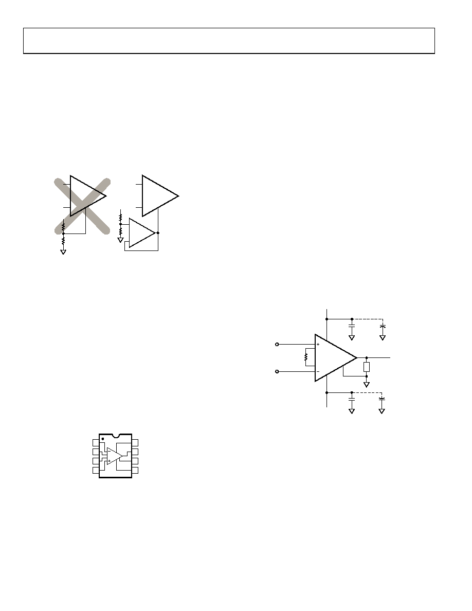
A 0.1 μF capacitor should be placed as close as possible to each
supply pin. As shown in Figure 59, a 10 μF tantalum capacitor
can be used farther away from the part. In most cases, it can be
shared by other precision integrated circuits.
AD8229
+VS
+IN
–IN
LOAD
RG
REF
0.1F
10F
0.1F
10F
–VS
VOUT
09
41
2-
0
61
Figure 59. Supply Decoupling, REF, and Output Referred to Local Ground
Reference Pin
The output voltage of the AD8229 is developed with respect to
the potential on the reference terminal. Care should be taken to
tie REF to the appropriate local ground.
相关PDF资料 |
PDF描述 |
|---|---|
| AD822BR-REEL | IC OPAMP GP R-R 1.9MHZ LP 8SOIC |
| AD8230YRZ-REEL7 | IC AMP CHOPPER R-R PREC 8SOIC |
| AD8231TCPZ-EP-R7 | IC INSTR AMP PROGR ENH 16LFCSP |
| AD8231WACPZ-RL | IC AMP INST RRO 2.7MHZ 16LFCSP |
| AD8235ACBZ-P7 | IC AMP INSTR RRIO 23KHZ 11WLCSP |
相关代理商/技术参数 |
参数描述 |
|---|---|
| AD8229HRZ-R7 | 功能描述:IC AMP INST LN 8SOIC RoHS:是 类别:集成电路 (IC) >> Linear - Amplifiers - Instrumentation 系列:- 其它有关文件:TS1854A View All Specifications 标准包装:50 系列:- 放大器类型:通用 电路数:4 输出类型:满摆幅 转换速率:0.25 V/µs 增益带宽积:630kHz -3db带宽:- 电流 - 输入偏压:16nA 电压 - 输入偏移:1000µV 电流 - 电源:162µA 电流 - 输出 / 通道:48mA 电压 - 电源,单路/双路(±):1.8 V ~ 6 V 工作温度:-40°C ~ 125°C 安装类型:表面贴装 封装/外壳:14-SOIC(0.154",3.90mm 宽) 供应商设备封装:14-SO 包装:管件 |
| AD8229XHDZ | 制造商:Analog Devices 功能描述:210 C CDIP IN AMP - Rail/Tube |
| AD822A/CHIPS | 制造商:未知厂家 制造商全称:未知厂家 功能描述:Voltage-Feedback Operational Amplifier |
| AD822ACHIPS | 制造商:AD 制造商全称:Analog Devices 功能描述:Single Supply, Rail-to-Rail Low Power FET-Input Op Amp |
| AD822AN | 功能描述:IC OPAMP GP R-R 1.9MHZ DUAL 8DIP RoHS:否 类别:集成电路 (IC) >> Linear - Amplifiers - Instrumentation 系列:- 标准包装:150 系列:- 放大器类型:音频 电路数:2 输出类型:- 转换速率:5 V/µs 增益带宽积:12MHz -3db带宽:- 电流 - 输入偏压:100nA 电压 - 输入偏移:500µV 电流 - 电源:6mA 电流 - 输出 / 通道:50mA 电压 - 电源,单路/双路(±):4 V ~ 32 V,±2 V ~ 16 V 工作温度:-40°C ~ 85°C 安装类型:表面贴装 封装/外壳:8-TSSOP(0.173",4.40mm 宽) 供应商设备封装:8-TSSOP 包装:管件 |
发布紧急采购,3分钟左右您将得到回复。