参数资料
| 型号: | AD8229HRZ |
| 厂商: | Analog Devices Inc |
| 文件页数: | 9/24页 |
| 文件大小: | 0K |
| 描述: | IC AMP INST LN 8SOIC |
| 标准包装: | 1 |
| 放大器类型: | 仪表 |
| 电路数: | 1 |
| 转换速率: | 22 V/µs |
| -3db带宽: | 15MHz |
| 电流 - 输入偏压: | 70nA |
| 电压 - 输入偏移: | 100µV |
| 电流 - 电源: | 6.7mA |
| 电流 - 输出 / 通道: | 35mA |
| 电压 - 电源,单路/双路(±): | ±4 V ~ 17 V |
| 工作温度: | -40°C ~ 175°C |
| 安装类型: | 表面贴装 |
| 封装/外壳: | 8-SOIC(0.154",3.90mm 宽) |
| 供应商设备封装: | 8-SO |
| 包装: | 管件 |
Data Sheet
AD8229
Rev. B | Page 17 of 24
THEORY OF OPERATION
A3
A1
A2
Q2
Q1
C1
C2
+IN
–IN
+VS
–VS
+VS
–VS
+VS
–VS
R3
5k
R4
5k
R5
5k
RG–
+VS
–VS
OUTPUT
REF
NODE 1
NODE 2
IB
COMPENSATION
IB
COMPENSATION
RG
VB
I
+VS
–VS
+VS
–VS
R6
5k
RG+
R2
3k
R1
3k
09412
-05
8
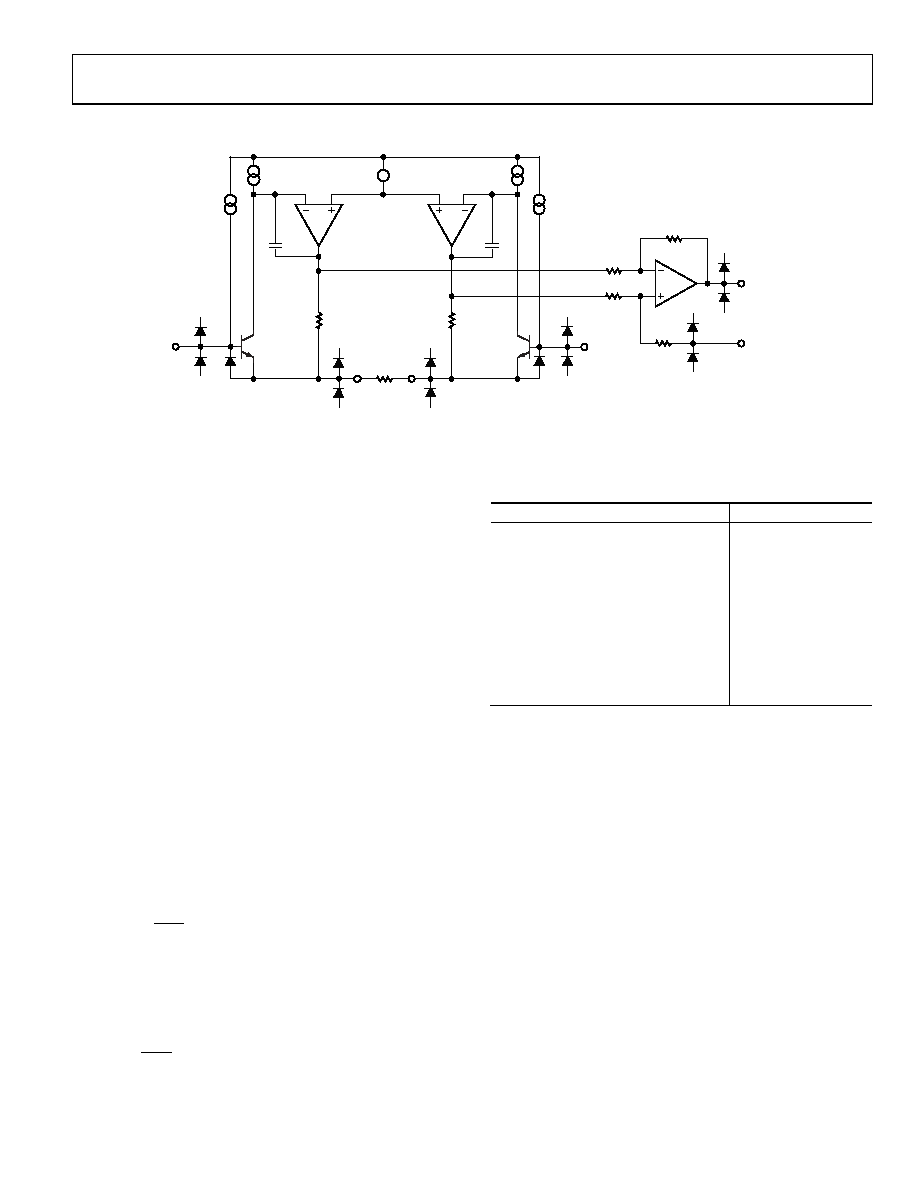
Figure 56. Simplified Schematic
ARCHITECTURE
The AD8229 is based on the classic 3-op-amp topology. This
topology has two stages: a preamplifier to provide differential
amplification followed by a difference amplifier that removes the
common-mode voltage and provides additional amplification.
Figure 56 shows a simplified schematic of the AD8229.
The first stage works as follows. To keep its two inputs matched,
Amplifier A1 must keep the collector of Q1 at a constant voltage. It
does this by forcing RG to be a precise diode drop from –IN.
Similarly, A2 forces RG+ to be a constant diode drop from +IN.
Therefore, a replica of the differential input voltage is placed
across the gain setting resistor, RG. The current that flows
through this resistance must also flow through the R1 and R2
resistors, creating a gained differential signal between the A2
and A1 outputs.
The second stage is a G = 1 difference amplifier, composed of
Amplifier A3 and the R3 through R6 resistors. This stage removes
the common-mode signal from the amplified differential signal.
The transfer function of the AD8229 is
VOUT = G × (VIN+ VIN) + VREF
where:
G
R
G
kΩ
6
1 +
=
GAIN SELECTION
Placing a resistor across the RG terminals sets the gain of the
using the following gain equation:
1
kΩ
6
=
G
RG
Table 5. Gains Achieved Using 1% Resistors
1% Standard Table Value of RG ()
Calculated Gain
6.04 k
1.993
1.5 k
5.000
665
10.02
316
19.99
121
50.59
60.4
100.34
30.1
200.34
12.1
496.9
6.04
994.4
3.01
1994.355
The AD8229 defaults to G = 1 when no gain resistor is used.
The tolerance and gain drift of the RG resistor should be added
to the AD8229’s specifications to determine the total gain accuracy
of the system. When the gain resistor is not used, gain error and
gain drift are minimal.
RG Power Dissipation
The AD8229 duplicates the differential voltage across its inputs
onto the RG resistor. The RG resistor size should be chosen to
handle the expected power dissipation.
REFERENCE TERMINAL
The output voltage of the AD8229 is developed with respect to
the potential on the reference terminal. This is useful when the
output signal must be offset to a precise midsupply level. For
example, a voltage source can be tied to the REF pin to level-
shift the output so that the AD8229 can drive a single-supply
ADC. The REF pin is protected with ESD diodes and should
not exceed either +VS or VS by more than 0.3 V.
相关PDF资料 |
PDF描述 |
|---|---|
| AD822BR-REEL | IC OPAMP GP R-R 1.9MHZ LP 8SOIC |
| AD8230YRZ-REEL7 | IC AMP CHOPPER R-R PREC 8SOIC |
| AD8231TCPZ-EP-R7 | IC INSTR AMP PROGR ENH 16LFCSP |
| AD8231WACPZ-RL | IC AMP INST RRO 2.7MHZ 16LFCSP |
| AD8235ACBZ-P7 | IC AMP INSTR RRIO 23KHZ 11WLCSP |
相关代理商/技术参数 |
参数描述 |
|---|---|
| AD8229HRZ-R7 | 功能描述:IC AMP INST LN 8SOIC RoHS:是 类别:集成电路 (IC) >> Linear - Amplifiers - Instrumentation 系列:- 其它有关文件:TS1854A View All Specifications 标准包装:50 系列:- 放大器类型:通用 电路数:4 输出类型:满摆幅 转换速率:0.25 V/µs 增益带宽积:630kHz -3db带宽:- 电流 - 输入偏压:16nA 电压 - 输入偏移:1000µV 电流 - 电源:162µA 电流 - 输出 / 通道:48mA 电压 - 电源,单路/双路(±):1.8 V ~ 6 V 工作温度:-40°C ~ 125°C 安装类型:表面贴装 封装/外壳:14-SOIC(0.154",3.90mm 宽) 供应商设备封装:14-SO 包装:管件 |
| AD8229XHDZ | 制造商:Analog Devices 功能描述:210 C CDIP IN AMP - Rail/Tube |
| AD822A/CHIPS | 制造商:未知厂家 制造商全称:未知厂家 功能描述:Voltage-Feedback Operational Amplifier |
| AD822ACHIPS | 制造商:AD 制造商全称:Analog Devices 功能描述:Single Supply, Rail-to-Rail Low Power FET-Input Op Amp |
| AD822AN | 功能描述:IC OPAMP GP R-R 1.9MHZ DUAL 8DIP RoHS:否 类别:集成电路 (IC) >> Linear - Amplifiers - Instrumentation 系列:- 标准包装:150 系列:- 放大器类型:音频 电路数:2 输出类型:- 转换速率:5 V/µs 增益带宽积:12MHz -3db带宽:- 电流 - 输入偏压:100nA 电压 - 输入偏移:500µV 电流 - 电源:6mA 电流 - 输出 / 通道:50mA 电压 - 电源,单路/双路(±):4 V ~ 32 V,±2 V ~ 16 V 工作温度:-40°C ~ 85°C 安装类型:表面贴装 封装/外壳:8-TSSOP(0.173",4.40mm 宽) 供应商设备封装:8-TSSOP 包装:管件 |
发布紧急采购,3分钟左右您将得到回复。