- 您现在的位置:买卖IC网 > PDF目录2063 > AD8332ACP-R2 (Analog Devices Inc)IC VGA DUAL W/PREAMP LN 32-LFCSP PDF资料下载
参数资料
| 型号: | AD8332ACP-R2 |
| 厂商: | Analog Devices Inc |
| 文件页数: | 19/56页 |
| 文件大小: | 0K |
| 描述: | IC VGA DUAL W/PREAMP LN 32-LFCSP |
| 产品变化通告: | Product Discontinuance 27/July/2010 |
| 标准包装: | 1 |
| 系列: | X-AMP® |
| 类型: | 可变增益放大器 |
| 应用: | 信号处理 |
| 安装类型: | 表面贴装 |
| 封装/外壳: | 32-VFQFN 裸露焊盘,CSP |
| 供应商设备封装: | 32-LFCSP-VQ(5x5) |
| 包装: | 标准包装 |
| 配用: | AD8332-EVALZ-ND - BOARD EVAL FOR AD8332 |
| 其它名称: | AD8332ACP-R2DKR |
第1页第2页第3页第4页第5页第6页第7页第8页第9页第10页第11页第12页第13页第14页第15页第16页第17页第18页当前第19页第20页第21页第22页第23页第24页第25页第26页第27页第28页第29页第30页第31页第32页第33页第34页第35页第36页第37页第38页第39页第40页第41页第42页第43页第44页第45页第46页第47页第48页第49页第50页第51页第52页第53页第54页第55页第56页
AD8331/AD8332/AD8334
Rev. G | Page 26 of 56
Active Impedance Matching
The LNA supports active impedance matching through an external
shunt feedback resistor from Pin LON to Pin INH. The input
resistance, RIN, is given in Equation 5, where A is the single-
ended gain of 4.5, and 6 kΩ is the unterminated input impedance.
IZ
IN
R
A
R
+
×
=
+
=
kΩ
33
kΩ
6
kΩ
6
1
(5)
CIZ is needed in series with RIZ because the dc levels at Pin LON
and Pin INH are unequal. Expressions for choosing RIZ in terms
at higher frequencies, where the loop gain is diminished, and
prevent peaking. Frequency response plots of the LNA are shown
130 MHz for matched input impedances of 50 Ω to 200 Ω and
declines at higher source impedances. The unterminated
bandwidth (when RIZ = ∞) is approximately 80 MHz.
Each output can drive external loads as low as 100 Ω in addition
to the 100 Ω input impedance of the VGA (200 Ω differential).
Capacitive loading up to 10 pF is permissible. All loads should
be ac-coupled. Typically, Pin LOP output is used as a single-ended
driver for auxiliary circuits, such as those used for Doppler
ultrasound imaging. Pin LON drives RIZ. Alternatively, a
differential external circuit can be driven from the two outputs
in addition to the active feedback termination. In both cases,
important stability considerations discussed in the Applications
Information section should be carefully observed.
The impedance at each LNA output is 5 Ω. A 0.4 dB reduction
in open circuit gain results when driving the VGA, and a 0.8 dB
reduction results with an additional 100 Ω load at the output.
The differential gain of the LNA is 6 dB higher. If the load is less
than 200 Ω on either side, a compensating load is recommended
on the opposite output.
LNA Noise
The input-referred voltage noise sets an important limit on
system performance. The short-circuit input voltage noise of
the LNA is 0.74 nV/√Hz or 0.82 nV/√Hz (at maximum gain),
including the VGA noise. The open circuit, current noise is
2.5 pA/√Hz. These measurements, taken without a feedback
resistor, provide the basis for calculating the input noise and
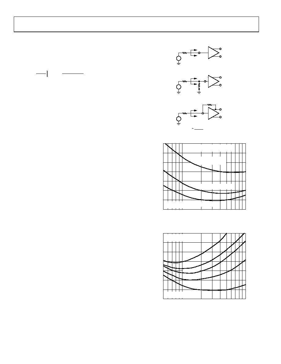
noise figure performance of the configurations in Figure 75.
results and the 4.1 dB noise figure (NF) measurement with the
input actively matched to a 50 Ω source. Unterminated (RIZ = ∞)
operation exhibits the lowest equivalent input noise and noise
figure. Figure 76 shows the noise figure vs. source resistance,
rising at low RS, where the LNA voltage noise is large compared
to the source noise, and again at high RS due to current noise.
The VGA input-referred voltage noise of 2.7 nV/√Hz is
included in all of the curves.
VOUT
UNTERMINATED
+
–
VIN
RIN
RS
VOUT
RESISTIVE TERMINATION
+
–
VIN
RIN
RS
VOUT
ACTIVE IMPEDANCE MATCH - RS = RIN
+
–
VIN
RIN
RIZ
1 + 4.5
RS
RIN =
03
19
9-
0
75
Figure 75. Input Configurations
7
6
5
4
3
2
1
0
50
100
1k
NO
IS
E
F
IG
UR
E
(
d
B)
RS ()
03
19
9-
0
76
INCLUDES NOISE OF VGA
RESISTIVE TERMINATION
(RS = RIN)
ACTIVE IMPEDANCE MATCH
UNTERMINATED
SIMULATION
Figure 76. Noise Figure vs. RS for Resistive,
Active Match, and Unterminated Inputs
7
6
5
4
3
2
1
0
50
100
1k
NO
IS
E
F
IG
UR
E
(
d
B)
RS ()
03
19
9-
0
77
INCLUDES NOISE OF VGA
RIN = 50
RIN = 75
RIN = 100
RIN = 200
RIZ = ∞
(SIMULATED RESULTS)
Figure 77. Noise Figure vs. RS for Various Fixed Values of RIN, Actively Matched
相关PDF资料 |
PDF描述 |
|---|---|
| AD8335ACPZ-REEL7 | IC AMP VGA QUAD 64LFCSP |
| AD8336ACPZ-WP | IC VGA GP SGL-ENDED 16-LFCSP |
| AD8337BCPZ-REEL7 | IC AMP VGA LOW NOISE 8-LFCSP |
| AD834AQ | IC MULTIPLIER 4-QUADRANT 8-CDIP |
| AD835AR | IC MULTIPLIER 4-QUADRANT 8-SOIC |
相关代理商/技术参数 |
参数描述 |
|---|---|
| AD8332ACP-REEL | 制造商:Analog Devices 功能描述:SP Amp Variable Gain Amp Dual 5.5V 32-Pin LFCSP EP T/R 制造商:Rochester Electronics LLC 功能描述: |
| AD8332ACP-REEL7 | 制造商:Analog Devices 功能描述:SP Amp Variable Gain Amp Dual 5.5V 32-Pin LFCSP EP T/R 制造商:Rochester Electronics LLC 功能描述: |
| AD8332ACPZ-R2 | 功能描述:IC AMP VGA PREAMP PROGR 32-LFCSP RoHS:是 类别:集成电路 (IC) >> 线性 - 放大器 - 专用 系列:X-AMP® 产品培训模块:Lead (SnPb) Finish for COTS Obsolescence Mitigation Program 标准包装:60 系列:- 类型:可变增益放大器 应用:CATV 安装类型:表面贴装 封装/外壳:20-WQFN 裸露焊盘 供应商设备封装:20-TQFN-EP(5x5) 包装:托盘 |
| AD8332ACPZ-R7 | 功能描述:IC AMP VAR GAIN 2CHAN 32-LFCSP RoHS:是 类别:集成电路 (IC) >> 线性 - 放大器 - 专用 系列:X-AMP® 产品培训模块:Lead (SnPb) Finish for COTS Obsolescence Mitigation Program 标准包装:60 系列:- 类型:可变增益放大器 应用:CATV 安装类型:表面贴装 封装/外壳:20-WQFN 裸露焊盘 供应商设备封装:20-TQFN-EP(5x5) 包装:托盘 |
| AD8332ACPZ-RL | 功能描述:IC AMP VAR GAIN 2CHAN 32LFCSP RoHS:是 类别:集成电路 (IC) >> 线性 - 放大器 - 专用 系列:X-AMP® 产品培训模块:Lead (SnPb) Finish for COTS Obsolescence Mitigation Program 标准包装:60 系列:- 类型:可变增益放大器 应用:CATV 安装类型:表面贴装 封装/外壳:20-WQFN 裸露焊盘 供应商设备封装:20-TQFN-EP(5x5) 包装:托盘 |
发布紧急采购,3分钟左右您将得到回复。