- 您现在的位置:买卖IC网 > PDF目录2063 > AD8332ACP-R2 (Analog Devices Inc)IC VGA DUAL W/PREAMP LN 32-LFCSP PDF资料下载
参数资料
| 型号: | AD8332ACP-R2 |
| 厂商: | Analog Devices Inc |
| 文件页数: | 25/56页 |
| 文件大小: | 0K |
| 描述: | IC VGA DUAL W/PREAMP LN 32-LFCSP |
| 产品变化通告: | Product Discontinuance 27/July/2010 |
| 标准包装: | 1 |
| 系列: | X-AMP® |
| 类型: | 可变增益放大器 |
| 应用: | 信号处理 |
| 安装类型: | 表面贴装 |
| 封装/外壳: | 32-VFQFN 裸露焊盘,CSP |
| 供应商设备封装: | 32-LFCSP-VQ(5x5) |
| 包装: | 标准包装 |
| 配用: | AD8332-EVALZ-ND - BOARD EVAL FOR AD8332 |
| 其它名称: | AD8332ACP-R2DKR |
第1页第2页第3页第4页第5页第6页第7页第8页第9页第10页第11页第12页第13页第14页第15页第16页第17页第18页第19页第20页第21页第22页第23页第24页当前第25页第26页第27页第28页第29页第30页第31页第32页第33页第34页第35页第36页第37页第38页第39页第40页第41页第42页第43页第44页第45页第46页第47页第48页第49页第50页第51页第52页第53页第54页第55页第56页
AD8331/AD8332/AD8334
Rev. G | Page 31 of 56
Gain Input
The GAIN pin is common to both channels of the AD8332. The
input impedance is nominally 10 MΩ, and a bypass capacitor
from 100 pF to 1 nF is recommended.
Parallel connected devices can be driven by a common voltage
source or DAC. Decoupling should take into account any band-
width considerations of the drive waveform, using the total
distributed capacitance.
If gain control noise in LO gain mode becomes a factor, main-
taining ≤15 nV/√Hz noise at the GAIN pin ensures satisfactory
noise performance. Internal noise prevails below 15 nV/√Hz at
the GAIN pin. Gain control noise is negligible in HI gain mode.
VCM Input
The common-mode voltage of Pin VCM, Pin VOL, and Pin VOH
defaults to 2.5 V dc. With output ac-coupled applications, the
VCM pin is unterminated; however, it must still be bypassed in
close proximity for ac grounding of internal circuitry. The VGA
outputs can be dc connected to a differential load, such as an
ADC. Common-mode output voltage levels between 1.5 V and
3.5 V can be realized at Pin VOH and Pin VOL by applying the
desired voltage at Pin VCM. DC-coupled operation is not
recommended when driving loads on a separate PC board.
The voltage on the VCM pin is sourced by an internal buffer
with an output impedance of 30 Ω and a ±2 mA default output
current (see Figure 83). If the VCM pin is driven from an external
source, its output impedance should be <<30 Ω, and its current
drive capability should be >>2 mA. If the VCM pins of several
devices are connected in parallel, the external buffer should be
capable of overcoming their collective output currents. When a
common-mode voltage other than 2.5 V is used, a voltage-
limiting resistor, RCLMP, is needed to protect against overload.
03
19
9-
0
83
VCM
NEW VCM
RO << 30
100pF
2mA MAX
30
0.1F
INTERNAL
CIRCUITRY
AC GROUNDING FOR
INTERNAL CIRCUITRY
Figure 83. VCM Interface
Logic Inputs—ENB, MODE, and HILO
The input impedance of all enable pins is nominally 25 kΩ and
can be pulled up to 5 V (a pull-up resistor is recommended) or
driven by any 3 V or 5 V logic families. The enable pin, ENB,
powers down the VGA; when pulled low, the VGA output voltages
are near ground. Multiple devices can be driven from a common
mation about circuit functions controlled by the enable pins.
Pin HILO is compatible with 3 V or 5 V CMOS logic families. It
is either connected to ground or pulled up to 5 V, depending on
the desired gain range and output noise.
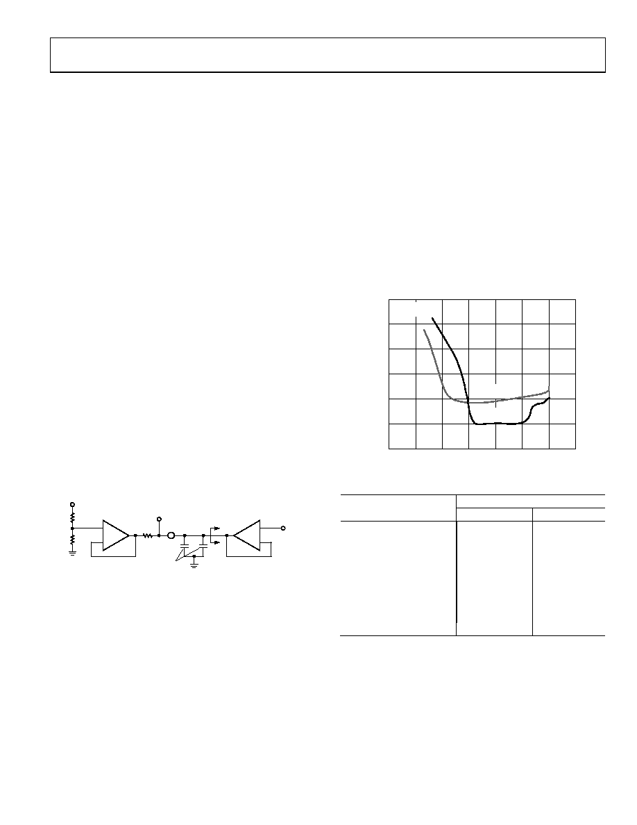
Optional Output Voltage Limiting
The RCLMP pin provides the user with a means to limit the
output voltage swing when used with loads that have no
provisions for prevention of input overdrive. The peak-to-peak
limited voltage is adjusted by a resistor to ground (see Table 8
for a list of several voltage levels and corresponding resistor
values). Unconnected, the default limiting level is 4.5 V p-p.
Note that third harmonic distortion increases as waveform
amplitudes approach clipping. For lowest distortion, the clamp level
should be set higher than the converter input span. A clamp level
of 1.5 V p-p is recommended for a 1 V p-p linear output range,
2.7 V p-p for a 2 V p-p range, or 1 V p-p for a 0.5 V p-p operation.
The best solution is determined experimentally. Figure 84 shows
third harmonic distortion as a function of the limiting level for
a 2 V p-p output signal. A wider limiting level is desirable in HI
gain mode.
–20
–30
–40
–50
–60
–70
–80
1.52.0
2.53.0
4.0
3.5
4.5
5.0
HD
3(
d
B
c)
CLAMP LIMIT LEVEL (V p-p)
03
19
9-
08
4
VGAIN = 0.75V
HILO = LO
HILO = HI
Figure 84. HD3 vs. Clamping Level for 2 V p-p Differential Input
Table 8. Clamp Resistor Values
Clamp Level (V p-p)
Clamp Resistor Value (kΩ)
HILO = LO
HILO = HI
0.5
1.21
1.0
2.74
2.21
1.5
4.75
4.02
2.0
7.5
6.49
2.5
11
9.53
3.0
16.9
14.7
3.5
26.7
23.2
4.0
49.9
39.2
4.4
100
73.2
Output Decoupling
When driving capacitive loads greater than about 10 pF, or long
circuit connections on other boards, an output network of resistors
and/or ferrite beads can be useful to ensure stability. These
components can be incorporated into a Nyquist filter such as
84.5 Ω. For example, all the evaluation boards for this series
incorporate 100 Ω in parallel with a 120 nH bead. Lower value
resistors are permissible for applications with nearby loads or
相关PDF资料 |
PDF描述 |
|---|---|
| AD8335ACPZ-REEL7 | IC AMP VGA QUAD 64LFCSP |
| AD8336ACPZ-WP | IC VGA GP SGL-ENDED 16-LFCSP |
| AD8337BCPZ-REEL7 | IC AMP VGA LOW NOISE 8-LFCSP |
| AD834AQ | IC MULTIPLIER 4-QUADRANT 8-CDIP |
| AD835AR | IC MULTIPLIER 4-QUADRANT 8-SOIC |
相关代理商/技术参数 |
参数描述 |
|---|---|
| AD8332ACP-REEL | 制造商:Analog Devices 功能描述:SP Amp Variable Gain Amp Dual 5.5V 32-Pin LFCSP EP T/R 制造商:Rochester Electronics LLC 功能描述: |
| AD8332ACP-REEL7 | 制造商:Analog Devices 功能描述:SP Amp Variable Gain Amp Dual 5.5V 32-Pin LFCSP EP T/R 制造商:Rochester Electronics LLC 功能描述: |
| AD8332ACPZ-R2 | 功能描述:IC AMP VGA PREAMP PROGR 32-LFCSP RoHS:是 类别:集成电路 (IC) >> 线性 - 放大器 - 专用 系列:X-AMP® 产品培训模块:Lead (SnPb) Finish for COTS Obsolescence Mitigation Program 标准包装:60 系列:- 类型:可变增益放大器 应用:CATV 安装类型:表面贴装 封装/外壳:20-WQFN 裸露焊盘 供应商设备封装:20-TQFN-EP(5x5) 包装:托盘 |
| AD8332ACPZ-R7 | 功能描述:IC AMP VAR GAIN 2CHAN 32-LFCSP RoHS:是 类别:集成电路 (IC) >> 线性 - 放大器 - 专用 系列:X-AMP® 产品培训模块:Lead (SnPb) Finish for COTS Obsolescence Mitigation Program 标准包装:60 系列:- 类型:可变增益放大器 应用:CATV 安装类型:表面贴装 封装/外壳:20-WQFN 裸露焊盘 供应商设备封装:20-TQFN-EP(5x5) 包装:托盘 |
| AD8332ACPZ-RL | 功能描述:IC AMP VAR GAIN 2CHAN 32LFCSP RoHS:是 类别:集成电路 (IC) >> 线性 - 放大器 - 专用 系列:X-AMP® 产品培训模块:Lead (SnPb) Finish for COTS Obsolescence Mitigation Program 标准包装:60 系列:- 类型:可变增益放大器 应用:CATV 安装类型:表面贴装 封装/外壳:20-WQFN 裸露焊盘 供应商设备封装:20-TQFN-EP(5x5) 包装:托盘 |
发布紧急采购,3分钟左右您将得到回复。