- 您现在的位置:买卖IC网 > PDF目录2063 > AD8332ACP-R2 (Analog Devices Inc)IC VGA DUAL W/PREAMP LN 32-LFCSP PDF资料下载
参数资料
| 型号: | AD8332ACP-R2 |
| 厂商: | Analog Devices Inc |
| 文件页数: | 26/56页 |
| 文件大小: | 0K |
| 描述: | IC VGA DUAL W/PREAMP LN 32-LFCSP |
| 产品变化通告: | Product Discontinuance 27/July/2010 |
| 标准包装: | 1 |
| 系列: | X-AMP® |
| 类型: | 可变增益放大器 |
| 应用: | 信号处理 |
| 安装类型: | 表面贴装 |
| 封装/外壳: | 32-VFQFN 裸露焊盘,CSP |
| 供应商设备封装: | 32-LFCSP-VQ(5x5) |
| 包装: | 标准包装 |
| 配用: | AD8332-EVALZ-ND - BOARD EVAL FOR AD8332 |
| 其它名称: | AD8332ACP-R2DKR |
第1页第2页第3页第4页第5页第6页第7页第8页第9页第10页第11页第12页第13页第14页第15页第16页第17页第18页第19页第20页第21页第22页第23页第24页第25页当前第26页第27页第28页第29页第30页第31页第32页第33页第34页第35页第36页第37页第38页第39页第40页第41页第42页第43页第44页第45页第46页第47页第48页第49页第50页第51页第52页第53页第54页第55页第56页
AD8331/AD8332/AD8334
Rev. G | Page 32 of 56
with gains less than 40 dB. The exact values of these components
can be selected empirically.
An antialiasing noise filter is typically used with an ADC. Filter
requirements are application dependent.
When the ADC resides on a separate board, the majority of
filter components should be placed nearby to suppress noise
picked up between boards and to mitigate charge kickback from
the ADC inputs. Any series resistance beyond that required for
output stability should be placed on the ADC board. Figure 85
shows a second-order, low-pass filter with a bandwidth of 20 MHz.
The capacitor is chosen in conjunction with the 10 pF input
capacitance of the ADC.
031
99
-08
5
18pF
OPTIONAL
BACKPLANE
0.1F
ADC
84.5
158
1.5H
Figure 85. 20 MHz Second-Order, Low-Pass Filter
DRIVING ADCs
The output drive accommodates a wide range of ADCs. The
noise floor requirements of the VGA depend on a number of
application factors, including bit resolution, sampling rate, full-
scale voltage, and the bandwidth of the noise/antialias filter. The
output noise floor and gain range can be adjusted by selecting
HI or LO gain mode.
The relative noise and distortion performance of the two gain
Figure 41. The 48 nV/√Hz noise floor of the LO gain mode is
suited to converters with higher sampling rates or resolutions
(such as 12 bits). Both gain modes can accommodate ADC full-
scale voltages as high as 4 V p-p. Because distortion performance
remains favorable for output voltages as high as 4 V p-p (see
Figure 36), it is possible to lower the output-referred noise even
further by using a resistive attenuator (or transformer) at the
output. The circuit in Figure 86 has an output full-scale range of
2 V p-p, a gain range of 10.5 dB to +37.5 dB, and an output
noise floor of 24 nV/√Hz, making it suitable for some 14-bit
ADC applications.
03
199
-08
6
ADC
AD6644
187
2:1
187
374
VOH
VOL
LPF
4V p-p DIFF,
48nV/ Hz
2V p-p DIFF,
24nV/ Hz
Figure 86. Adjusting the Noise Floor for 14-Bit ADCs
OVERLOAD
These devices respond gracefully to large signals that overload
its input stage and to normal signals that overload the VGA
when the gain is set unexpectedly high. Each stage is designed
for clean-limited overload waveforms and fast recovery when
gain setting or input amplitude is reduced.
Signals larger than ±275 mV at the LNA input are clipped to
5 V p-p differential prior to the input of the VGA. Figure 48
shows the response to a 1 V p-p input burst. The symmetric
overload waveform is important for applications, such as CW
Doppler ultrasound, where the spectrum of the LNA outputs
during overload is critical. The input stage is also designed to
accommodate signals as high as ±2.5 V without triggering the
slow-settling ESD input protection diodes.
Both stages of the VGA are susceptible to overload. Post-
amplifier limiting is more common and results in the clean-
limited output characteristics found in Figure 49. Recovery is fast in
all cases. The graph in Figure 87 summarizes the combinations of
input signal and gain that lead to the different types of overload.
03
19
9-
0
8
7
G
A
IN
(d
B
)
1m
LO GAIN
MODE
15mV
–4.5
25mV
L
N
A
O
V
E
R
L
O
A
D
X-AMP
OVERLOAD
POSTAMP
OVERLOAD
X-AMP
OVERLOAD
POSTAMP
OVERLOAD
29dB
43.5
INPUT AMPLITUDE (V)
0.275
0.1
10m
24.5dB
G
A
IN
(d
B
)
HI GAIN
MODE
4mV
7.5
25mV
L
N
A
O
V
E
R
L
O
A
D
41dB
56.5
INPUT AMPLITUDE (V)
24.5dB
1
1m
0.275
0.1
10m
1
Figure 87. Overload Gain and Signal Conditions
The clamp interface mentioned in the Output Clamping section
controls the maximum output swing of the postamp and its
overload response. When the clamp feature is not used, the
output level defaults to approximately 4.5 V p-p differential
centered at 2.5 V common mode. When other common-mode
levels are set through the VCM pin, the value of RCLMP should be
selected for graceful overload. A value of 8.3 kΩ or less is
recommended for 1.5 V or 3.5 V common-mode levels (7.2 kΩ
for HI gain mode). This limits the output swing to just above
2 V p-p differential.
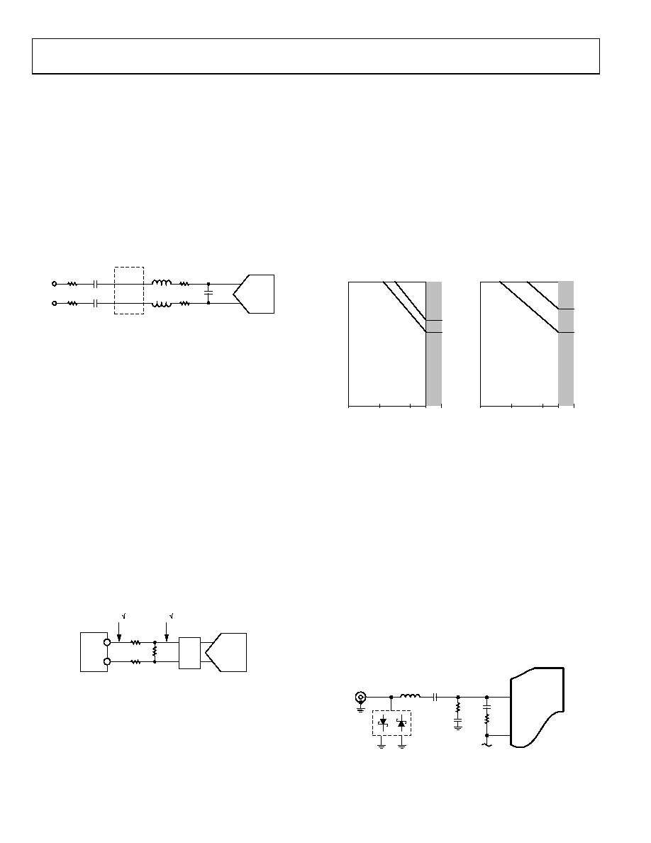
OPTIONAL INPUT OVERLOAD PROTECTION
Applications in which high transients are applied to the LNA
input can benefit from the use of clamp diodes. A pair of back-
to-back Schottky diodes can reduce these transients to manageable
levels. Figure 88 illustrates how such a diode protection scheme
can be connected.
03
19
9-
0
88
20
19
4
3
2
LON
VPSL
INH
COMM
ENBL
0.1F
FB
RSH
CIZ
RIZ
CSH
2
3
1
OPTIONAL
SCHOTTKY
OVERLOAD
CLAMP
BAS40-04
Figure 88. Input Overload Clamping
相关PDF资料 |
PDF描述 |
|---|---|
| AD8335ACPZ-REEL7 | IC AMP VGA QUAD 64LFCSP |
| AD8336ACPZ-WP | IC VGA GP SGL-ENDED 16-LFCSP |
| AD8337BCPZ-REEL7 | IC AMP VGA LOW NOISE 8-LFCSP |
| AD834AQ | IC MULTIPLIER 4-QUADRANT 8-CDIP |
| AD835AR | IC MULTIPLIER 4-QUADRANT 8-SOIC |
相关代理商/技术参数 |
参数描述 |
|---|---|
| AD8332ACP-REEL | 制造商:Analog Devices 功能描述:SP Amp Variable Gain Amp Dual 5.5V 32-Pin LFCSP EP T/R 制造商:Rochester Electronics LLC 功能描述: |
| AD8332ACP-REEL7 | 制造商:Analog Devices 功能描述:SP Amp Variable Gain Amp Dual 5.5V 32-Pin LFCSP EP T/R 制造商:Rochester Electronics LLC 功能描述: |
| AD8332ACPZ-R2 | 功能描述:IC AMP VGA PREAMP PROGR 32-LFCSP RoHS:是 类别:集成电路 (IC) >> 线性 - 放大器 - 专用 系列:X-AMP® 产品培训模块:Lead (SnPb) Finish for COTS Obsolescence Mitigation Program 标准包装:60 系列:- 类型:可变增益放大器 应用:CATV 安装类型:表面贴装 封装/外壳:20-WQFN 裸露焊盘 供应商设备封装:20-TQFN-EP(5x5) 包装:托盘 |
| AD8332ACPZ-R7 | 功能描述:IC AMP VAR GAIN 2CHAN 32-LFCSP RoHS:是 类别:集成电路 (IC) >> 线性 - 放大器 - 专用 系列:X-AMP® 产品培训模块:Lead (SnPb) Finish for COTS Obsolescence Mitigation Program 标准包装:60 系列:- 类型:可变增益放大器 应用:CATV 安装类型:表面贴装 封装/外壳:20-WQFN 裸露焊盘 供应商设备封装:20-TQFN-EP(5x5) 包装:托盘 |
| AD8332ACPZ-RL | 功能描述:IC AMP VAR GAIN 2CHAN 32LFCSP RoHS:是 类别:集成电路 (IC) >> 线性 - 放大器 - 专用 系列:X-AMP® 产品培训模块:Lead (SnPb) Finish for COTS Obsolescence Mitigation Program 标准包装:60 系列:- 类型:可变增益放大器 应用:CATV 安装类型:表面贴装 封装/外壳:20-WQFN 裸露焊盘 供应商设备封装:20-TQFN-EP(5x5) 包装:托盘 |
发布紧急采购,3分钟左右您将得到回复。