- 您现在的位置:买卖IC网 > PDF目录6065 > AD8555ACPZ-REEL7 (Analog Devices Inc)IC AMP CHOPPER 2MHZ 10MA 16LFCSP PDF资料下载
参数资料
| 型号: | AD8555ACPZ-REEL7 |
| 厂商: | Analog Devices Inc |
| 文件页数: | 15/28页 |
| 文件大小: | 0K |
| 描述: | IC AMP CHOPPER 2MHZ 10MA 16LFCSP |
| 标准包装: | 1 |
| 系列: | DigiTrim® |
| 放大器类型: | 断路器(零漂移) |
| 电路数: | 1 |
| 转换速率: | 1.2 V/µs |
| 增益带宽积: | 2MHz |
| 电流 - 输入偏压: | 16nA |
| 电压 - 输入偏移: | 2µV |
| 电流 - 电源: | 2mA |
| 电流 - 输出 / 通道: | 10mA |
| 电压 - 电源,单路/双路(±): | 2.7 V ~ 5.5 V |
| 工作温度: | -40°C ~ 125°C |
| 安装类型: | 表面贴装 |
| 封装/外壳: | 16-VQFN 裸露焊盘,CSP |
| 供应商设备封装: | 16-LFCSP-VQ |
| 包装: | 标准包装 |
| 产品目录页面: | 771 (CN2011-ZH PDF) |
| 其它名称: | AD8555ACPZ-REEL7DKR |
第1页第2页第3页第4页第5页第6页第7页第8页第9页第10页第11页第12页第13页第14页当前第15页第16页第17页第18页第19页第20页第21页第22页第23页第24页第25页第26页第27页第28页
AD8555
Rev. A | Page 22 of 28
IN01
IN02
IN03
IN04
IN05
IN06
IN07
IN08
IN09
IN10
IN11
IN12
IN13
IN14
IN15
IN16
IN17
IN18
VA0
VA1
VA2
VB0
VB1
VB2
VB3
VB4
VB5
VB6
VC0
VC1
VC2
VC3
VC4
VC5
VC6
VC7
EOR18
OUT
I0
DOT_SUM
PAR_SUM
PFUSE
MFUSE
IN1
IN2
EOR2
AND2
IN1
IN2
PARITY_ERROR
I1
OUT
I2
OUT
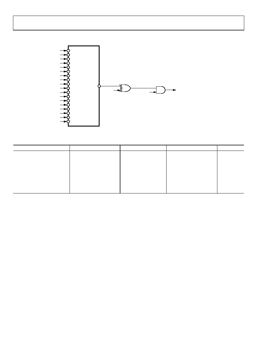
04598-0-004
Figure 52. Functional Circuit of AD8555 Parity Check
Table 13. Examples of DAT_SUM
Second Stage Gain Code
First Stage Gain Code
Output Offset Code
Number of Bits with 1
DAT_SUM
000
000 0000
0000 0000
0
000
000 0000
1000 0000
1
000
000 0000
1000 0001
2
0
000
000 0001
0000 0000
1
000
100 0001
0000 0000
2
0
001
000 0000
0000 0000
1
001
000 0001
1000 0000
3
1
111
111 1111
1111 1111
18
0
VA0 to VA2 is the 3-bit control signal for the second stage gain,
VB0 to VB6 is the 7-bit control signal for the first stage gain,
and VC0 to VC7 is the 8-bit control signal for the output offset.
PFUSE is the signal from the parity fuse, and MFUSE is the
signal from the master fuse.
The function of the 2-input AND gate (cell and2) is to ignore
the output of the parity circuit (signal PAR_SUM) when the
master fuse has not been blown. PARITY_ERROR is set to 0
when MFUSE = 0. In the simulation mode, for example, parity
check is disabled. After the master fuse has been blown, i.e.,
after the AD8555 has been programmed, the output from the
parity circuit (signal PAR_SUM) is fed to PARITY_ERROR.
When PARITY_ERROR is 0, the AD8555 behaves as a pro-
grammed amplifier. When PARITY_ERROR is 1, a parity error
has been detected, and VOUT is connected to VSS.
The 18-bit data signal (VA0 to VA2, VB0 to VB6, and VC0 to
VC7) is fed to an 18-input exclusive-OR gate (Cell EOR18). The
output of Cell EOR18 is the signal DAT_SUM. DAT_SUM = 0 if
there is an even number of 1s in the 18-bit word; DAT_SUM =
1 if there is an odd number of 1s in the 18-bit word. Examples
are given in Table 13.
相关PDF资料 |
PDF描述 |
|---|---|
| TSW-109-08-G-S-RA | CONN HEADER 9POS .100 SGL R/A AU |
| AWH30A-0202-T-R | CONN HEADER 30POS RT ANG GOLD |
| TSW-122-07-T-S | CONN HEADER 22POS .100" SNGL TIN |
| AWH40G-0202-T-R | CONN HEADER 40POS VERT GOLD |
| TSW-122-06-T-S | CONN HEADER 22POS .100" SNGL TIN |
相关代理商/技术参数 |
参数描述 |
|---|---|
| AD8555ACPZ-REEL71 | 制造商:AD 制造商全称:Analog Devices 功能描述:Zero-Drift, Digitally Programmable Sensor Signal Amplifier |
| AD8555AR | 制造商:Analog Devices 功能描述:SP Amp Current Sense Amp Single R-R I/O 5.5V 8-Pin SOIC N Tube 制造商:Analog Devices 功能描述:2.7V to 5.5V 1 2MHz vAv 8SOIC Bulk 制造商:Analog Devices 功能描述:AMP Z-DRIFT PROG GAIN 8555 SOIC8 |
| AD8555AR-EVAL | 制造商:Analog Devices 功能描述:Evaluation Board For Zero-Drift, Digitally Programmable Sensor Signal Amplifier |
| AD8555AR-REEL | 制造商:Analog Devices 功能描述:SP Amp Current Sense Amp Single R-R I/O 5.5V 8-Pin SOIC N T/R |
| AD8555AR-REEL7 | 制造商:Analog Devices 功能描述:SP Amp Current Sense Amp Single R-R I/O 5.5V 8-Pin SOIC N T/R |
发布紧急采购,3分钟左右您将得到回复。