参数资料
| 型号: | AD8659ARZ |
| 厂商: | Analog Devices Inc |
| 文件页数: | 11/24页 |
| 文件大小: | 0K |
| 描述: | IC OPAMP RRIO 18V CMOS 14SOIC |
| 标准包装: | 56 |
| 放大器类型: | 通用 |
| 电路数: | 4 |
| 输出类型: | 满摆幅 |
| 转换速率: | 0.07 V/µs |
| 增益带宽积: | 200kHz |
| 电流 - 输入偏压: | 5pA |
| 电压 - 输入偏移: | 350µV |
| 电流 - 电源: | 18µA |
| 电流 - 输出 / 通道: | 12mA |
| 电压 - 电源,单路/双路(±): | 2.7 V ~ 18 V,±1.35 V ~ 9 V |
| 工作温度: | -40°C ~ 125°C |
| 安装类型: | 表面贴装 |
| 封装/外壳: | 14-SOIC(0.154",3.90mm 宽) |
| 供应商设备封装: | 14-SO |
| 包装: | 管件 |
Data Sheet
AD8657/AD8659
Rev. B | Page 19 of 24
APPLICATIONS INFORMATION
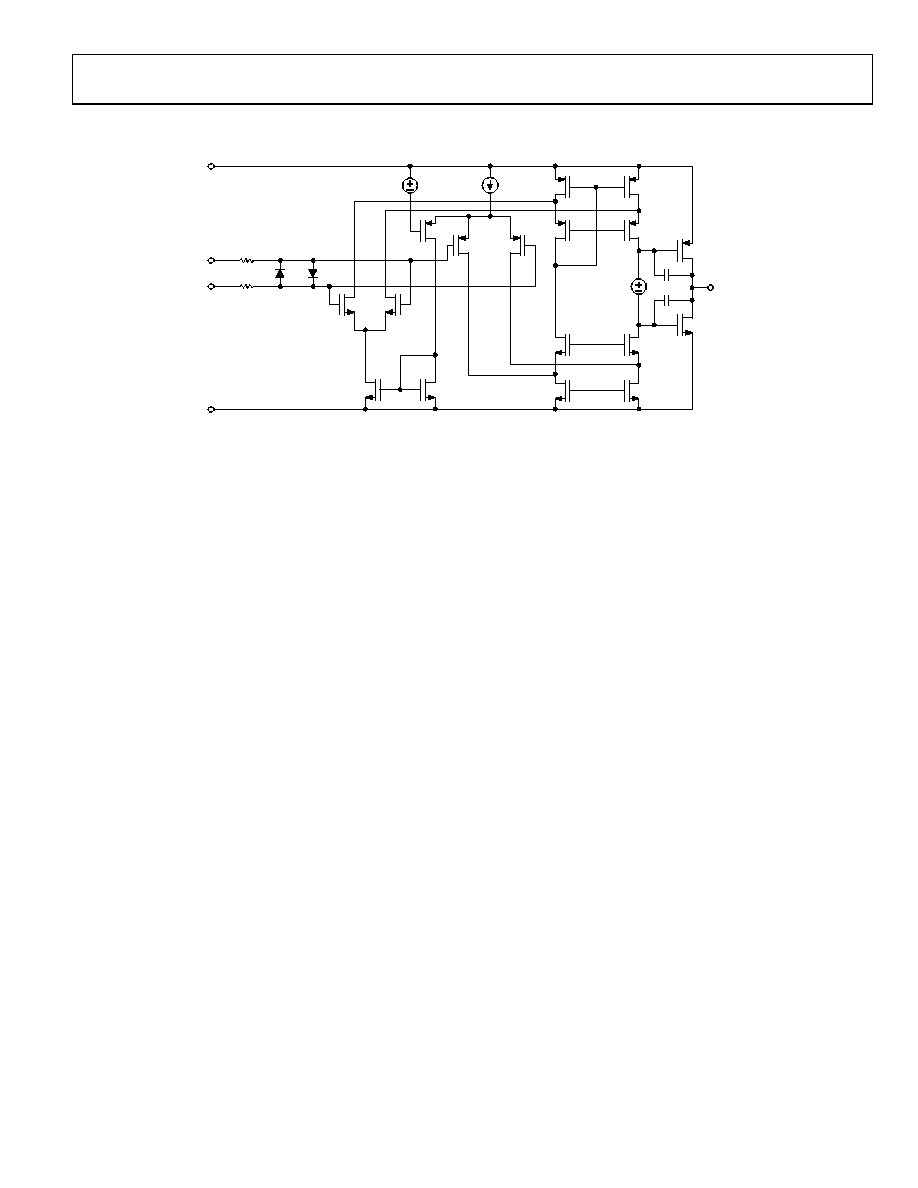
V+
V–
+IN x
R1
D1
D2
M1
M2
M7
M6
M3
M4
M5
VB1
M8
M10
M9
M16
M17
M11
VB2
OUT x
M12
M14
M13
M15
I1
R2
–IN x
08804-
056
Figure 68. Simplified Schematic
The AD8657/AD8659 are low power, rail-to-rail input and output
precision CMOS amplifiers that operate over a wide supply
Analog Devices DigiTrim technique to achieve a higher degree
of precision than is available from other CMOS amplifiers. The
DigiTrim technique is a method of trimming the offset voltage
of an amplifier after assembly. The advantage of post-package
trimming is that it corrects any shifts in offset voltage caused by
mechanical stresses of assembly.
The AD8657/AD8659 also employ unique input and output
stages to achieve a rail-to-rail input and output range with a
very low supply current.
INPUT STAGE
The input stage comprises two differential transistor pairs, an
NMOS pair (M1, M2) and a PMOS pair (M3, M4). The input
common-mode voltage determines which differential pair turns
on and is more active than the other.
The PMOS differential pair is active when the input voltage
approaches and reaches the lower supply rail. The NMOS pair
is needed for input voltages up to and including the upper supply
rail. This topology allows the amplifier to maintain a wide
dynamic input voltage range and to maximize signal swing to
both supply rails.
For the majority of the input common-mode voltage range, the
PMOS differential pair is active. Differential pairs commonly
exhibit different offset voltages. The handoff from one pair to the
other creates a step-like characteristic that is visible in the VOS vs.
inherent in all rail-to-rail amplifiers that use the dual differential
pair topology. Therefore, always choose a common-mode voltage
that does not include the region of handoff from one input
differential pair to the other.
Additional steps in the VOS vs. VCM curves are also visible as the
input common-mode voltage approaches the power supply rails.
These changes are a result of the load transistors (M8, M9, M14,
and M15) running out of headroom. As the load transistors are
forced into the triode region of operation, the mismatch of their
drain impedances contributes to the offset voltage of the amplifier.
This problem is exacerbated at high temperatures due to the
decrease in the threshold voltage of the input transistors (see
Figure 14, Figure 15, Figure 17, and Figure 18 for typical perfor-
mance data).
Current Source I1 drives the PMOS transistor pair. As the input
common-mode voltage approaches the upper rail, I1 is steered
away from the PMOS differential pair through the M5 transistor.
The bias voltage, VB1 (see Figure 68), controls the point where this
transfer occurs. M5 diverts the tail current into a current mirror
consisting of the M6 and M7 transistors. The output of the current
mirror then drives the NMOS pair. Note that the activation of
this current mirror causes a slight increase in supply current at
high common-mode voltages (see Figure 28 and Figure 31 for
more details).
low voltage MOS devices for their differential inputs. These low
voltage MOS devices offer excellent noise and bandwidth per
unit of current. Each differential input pair is protected by proprie-
tary regulation circuitry (not shown in the simplified schematic).
The regulation circuitry consists of a combination of active
devices that maintain the proper voltages across the input pairs
during normal operation and passive clamping devices that protect
the amplifier during fast transients. However, these passive
clamping devices begin to forward bias as the common-mode
voltage approaches either power supply rail, thereby causing an
increase in the input bias current (see Figure 20 and Figure 23).
The input devices are also protected from large differential
input voltages by clamp diodes (D1 and D2). These diodes are
buffered from the inputs with two 10 k resistors (R1 and R2).
The differential diodes turn on whenever the differential voltage
exceeds approximately 600 mV; in this condition, the differential
input resistance drops to 20 k.
相关PDF资料 |
PDF描述 |
|---|---|
| AD848JRZ-REEL | IC OPAMP GP 175MHZ LP 32MA 8SOIC |
| PEC26DBDN | CONN HEADER .100 DUAL R/A 52POS |
| PEC26DAHN | CONN HEADER .100 DUAL STR 52POS |
| TPS-15 | FUSE TELPOWER 15A 170VDC |
| TPS-10 | FUSE TELPOWER 10A 170VDC |
相关代理商/技术参数 |
参数描述 |
|---|---|
| AD8659ARZ_PROMO | 制造商:Analog Devices 功能描述:OP AMP QUAD 18V RRIO 230KH |
| AD8659ARZ-R7 | 功能描述:IC OPAMP RRIO 18V CMOS 14SOIC RoHS:是 类别:集成电路 (IC) >> Linear - Amplifiers - Instrumentation 系列:- 标准包装:1,000 系列:- 放大器类型:电压反馈 电路数:4 输出类型:满摆幅 转换速率:33 V/µs 增益带宽积:20MHz -3db带宽:30MHz 电流 - 输入偏压:2nA 电压 - 输入偏移:3000µV 电流 - 电源:2.5mA 电流 - 输出 / 通道:30mA 电压 - 电源,单路/双路(±):4.5 V ~ 16.5 V,±2.25 V ~ 8.25 V 工作温度:-40°C ~ 85°C 安装类型:表面贴装 封装/外壳:14-SOIC(0.154",3.90mm 宽) 供应商设备封装:14-SOIC 包装:带卷 (TR) |
| AD8659ARZ-RL | 功能描述:IC OPAMP RRIO 18V CMOS 14SOIC RoHS:是 类别:集成电路 (IC) >> Linear - Amplifiers - Instrumentation 系列:- 标准包装:1,000 系列:- 放大器类型:电压反馈 电路数:4 输出类型:满摆幅 转换速率:33 V/µs 增益带宽积:20MHz -3db带宽:30MHz 电流 - 输入偏压:2nA 电压 - 输入偏移:3000µV 电流 - 电源:2.5mA 电流 - 输出 / 通道:30mA 电压 - 电源,单路/双路(±):4.5 V ~ 16.5 V,±2.25 V ~ 8.25 V 工作温度:-40°C ~ 85°C 安装类型:表面贴装 封装/外壳:14-SOIC(0.154",3.90mm 宽) 供应商设备封装:14-SOIC 包装:带卷 (TR) |
| AD8661 | 制造商:AD 制造商全称:Analog Devices 功能描述:Low Noise, Precision 16 V CMOS, Rail-to-Rail Operational Amplifiers |
| AD8661_06 | 制造商:AD 制造商全称:Analog Devices 功能描述:Low Noise, Precision 16 V CMOS, Rail-to-Rail Operational Amplifiers |
发布紧急采购,3分钟左右您将得到回复。