参数资料
| 型号: | AD8659ARZ |
| 厂商: | Analog Devices Inc |
| 文件页数: | 15/24页 |
| 文件大小: | 0K |
| 描述: | IC OPAMP RRIO 18V CMOS 14SOIC |
| 标准包装: | 56 |
| 放大器类型: | 通用 |
| 电路数: | 4 |
| 输出类型: | 满摆幅 |
| 转换速率: | 0.07 V/µs |
| 增益带宽积: | 200kHz |
| 电流 - 输入偏压: | 5pA |
| 电压 - 输入偏移: | 350µV |
| 电流 - 电源: | 18µA |
| 电流 - 输出 / 通道: | 12mA |
| 电压 - 电源,单路/双路(±): | 2.7 V ~ 18 V,±1.35 V ~ 9 V |
| 工作温度: | -40°C ~ 125°C |
| 安装类型: | 表面贴装 |
| 封装/外壳: | 14-SOIC(0.154",3.90mm 宽) |
| 供应商设备封装: | 14-SO |
| 包装: | 管件 |
AD8657/AD8659
Data Sheet
Rev. B | Page 22 of 24
EMI REJECTION RATIO
Circuit performance is often adversely affected by high frequency
electromagnetic interference (EMI). In the event where signal
strength is low and transmission lines are long, an op amp must
accurately amplify the input signals. However, all op amp pins—
the noninverting input, inverting input, positive supply, negative
supply, and output pins—are susceptible to EMI signals. These
high frequency signals are coupled into an op amp by various
means such as conduction, near field radiation, or far field radi-
ation. For example, wires and PCB traces can act as antennas and
pick up high frequency EMI signals.
amplify EMI or RF signals because of their relatively low
bandwidth. However, due to the nonlinearities of the input
devices, op amps can rectify these out-of-band signals. When
these high frequency signals are rectified, they appear as a dc
offset at the output.
To describe the ability of the AD8657/AD8659 to perform as
intended in the presence of an electromagnetic energy, the
electromagnetic interference rejection ratio (EMIRR) of the
the Specifications section. A mathematical method of
measuring EMIRR is defined as follows:
EMIRR = 20 log (VIN_PEAK/ΔVOS)
20
40
60
80
100
120
140
10M
100M
1G
10G
E
M
IRR
(
d
B)
FREQUENCY (Hz)
VIN = 100mVPEAK
VSY = 2.7V TO 18V
08804-
071
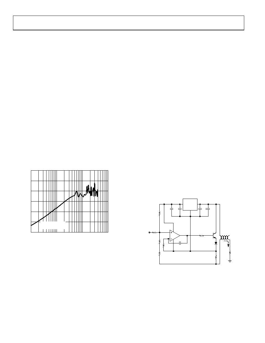
Figure 77. EMIRR vs. Frequency
4 mA TO 20 mA PROCESS CONTROL CURRENT
LOOP TRANSMITTER—AD8657
The 2-wire current transmitters are often used in distributed
control systems and process control applications to transmit
analog signals between sensors and process controllers. Figure 78
shows a 4 mA to 20 mA current loop transmitter.
The transmitter powers directly from the control loop power
supply, and the current in the loop carries signal from 4 mA to
20 mA. Thus, 4 mA establishes the baseline current budget within
which the circuit must operate. Using the AD8657 is an excellent
choice due to its low supply current of 34 μA per amplifier over
temperature and supply voltage. The current transmitter controls
the current flowing in the loop, where a zero-scale input signal
is represented by 4 mA of current and a full-scale input signal
is represented by 20 mA. The transmitter also floats from the
control loop power supply, VDD, while signal ground is in the
receiver. The loop current is measured at the load resistor, RL,
at the receiver side.
At a zero-scale input, a current of VREF/RNULL flows through R.
This creates a current flowing through the sense resistor, ISENSE,
determined by the following equation (see Figure 78 for details):
ISENSE,MIN = (VREF × R)/(RNULL × RSENSE)
With a full-scale input voltage, current flowing through R is
increased by the full-scale change in VIN/RSPAN. This creates an
increase in the current flowing through the sense resistor.
ISENSE,DELTA = (Full-Scale Change in VIN × R)/(RSPAN × RSENSE)
Therefore
ISENSE,MAX = ISENSE,MIN + ISENSE,DELTA
When R >> RSENSE, the current through the load resistor at the
receiver side is almost equivalent to ISENSE.
Figure 78 is designed for a full-scale input voltage of 5 V. At 0 V
of input, loop current is 3.5 mA; and at a full scale of 5 V, the
loop current is 21 mA. This allows software calibration to fine
tune the current loop to the 4 mA to 20 mA range.
The AD8657 and ADR125 both consume only 160 A quiescent
current, making 3.34 mA current available to power additional
signal conditioning circuitry or to power a bridge circuit.
RL
100
VDD
18V
C2
10F
C3
0.1F
C1
390pF
C4
0.1F
R4
3.3k
Q1
D1
4mA
TO
20mA
R3
1.2k
RNULL
1M
1%
VREF
RSPAN
200k
1%
VIN
0V TO 5V
R1
68k
1%
R2
2k
1%
NOTES
1. R1 + R2 = R.
1/2
AD8657
C5
10F
RSENSE
100
1%
08804-
060
VOUT
GND
ADR125
VIN
Figure 78. 4 mA to 20 mA Current Loop Transmitter
相关PDF资料 |
PDF描述 |
|---|---|
| AD848JRZ-REEL | IC OPAMP GP 175MHZ LP 32MA 8SOIC |
| PEC26DBDN | CONN HEADER .100 DUAL R/A 52POS |
| PEC26DAHN | CONN HEADER .100 DUAL STR 52POS |
| TPS-15 | FUSE TELPOWER 15A 170VDC |
| TPS-10 | FUSE TELPOWER 10A 170VDC |
相关代理商/技术参数 |
参数描述 |
|---|---|
| AD8659ARZ_PROMO | 制造商:Analog Devices 功能描述:OP AMP QUAD 18V RRIO 230KH |
| AD8659ARZ-R7 | 功能描述:IC OPAMP RRIO 18V CMOS 14SOIC RoHS:是 类别:集成电路 (IC) >> Linear - Amplifiers - Instrumentation 系列:- 标准包装:1,000 系列:- 放大器类型:电压反馈 电路数:4 输出类型:满摆幅 转换速率:33 V/µs 增益带宽积:20MHz -3db带宽:30MHz 电流 - 输入偏压:2nA 电压 - 输入偏移:3000µV 电流 - 电源:2.5mA 电流 - 输出 / 通道:30mA 电压 - 电源,单路/双路(±):4.5 V ~ 16.5 V,±2.25 V ~ 8.25 V 工作温度:-40°C ~ 85°C 安装类型:表面贴装 封装/外壳:14-SOIC(0.154",3.90mm 宽) 供应商设备封装:14-SOIC 包装:带卷 (TR) |
| AD8659ARZ-RL | 功能描述:IC OPAMP RRIO 18V CMOS 14SOIC RoHS:是 类别:集成电路 (IC) >> Linear - Amplifiers - Instrumentation 系列:- 标准包装:1,000 系列:- 放大器类型:电压反馈 电路数:4 输出类型:满摆幅 转换速率:33 V/µs 增益带宽积:20MHz -3db带宽:30MHz 电流 - 输入偏压:2nA 电压 - 输入偏移:3000µV 电流 - 电源:2.5mA 电流 - 输出 / 通道:30mA 电压 - 电源,单路/双路(±):4.5 V ~ 16.5 V,±2.25 V ~ 8.25 V 工作温度:-40°C ~ 85°C 安装类型:表面贴装 封装/外壳:14-SOIC(0.154",3.90mm 宽) 供应商设备封装:14-SOIC 包装:带卷 (TR) |
| AD8661 | 制造商:AD 制造商全称:Analog Devices 功能描述:Low Noise, Precision 16 V CMOS, Rail-to-Rail Operational Amplifiers |
| AD8661_06 | 制造商:AD 制造商全称:Analog Devices 功能描述:Low Noise, Precision 16 V CMOS, Rail-to-Rail Operational Amplifiers |
发布紧急采购,3分钟左右您将得到回复。