- 您现在的位置:买卖IC网 > PDF目录10531 > AD9219ABCPZ-40 (Analog Devices Inc)IC ADC 10BIT SRL 40MSPS 64LFCSP PDF资料下载
参数资料
| 型号: | AD9219ABCPZ-40 |
| 厂商: | Analog Devices Inc |
| 文件页数: | 30/56页 |
| 文件大小: | 0K |
| 描述: | IC ADC 10BIT SRL 40MSPS 64LFCSP |
| 标准包装: | 1 |
| 位数: | 10 |
| 采样率(每秒): | 40M |
| 数据接口: | 串行,SPI? |
| 转换器数目: | 4 |
| 功率耗散(最大): | 313mW |
| 电压电源: | 模拟和数字 |
| 工作温度: | -40°C ~ 85°C |
| 安装类型: | 表面贴装 |
| 封装/外壳: | 48-VFQFN 裸露焊盘,CSP |
| 供应商设备封装: | 48-LFCSP-VQ(7x7) |
| 包装: | 托盘 |
| 输入数目和类型: | 8 个单端,单极;4 个差分,单极 |
第1页第2页第3页第4页第5页第6页第7页第8页第9页第10页第11页第12页第13页第14页第15页第16页第17页第18页第19页第20页第21页第22页第23页第24页第25页第26页第27页第28页第29页当前第30页第31页第32页第33页第34页第35页第36页第37页第38页第39页第40页第41页第42页第43页第44页第45页第46页第47页第48页第49页第50页第51页第52页第53页第54页第55页第56页
AD9219
Data Sheet
Rev. E | Page 36 of 56
Power and Ground Recommendations
When connecting power to the AD9219, it is recommended
that two separate 1.8 V supplies be used: one for analog (AVDD)
and one for digital (DRVDD). If only one supply is available, it
should be routed to the AVDD first and then tapped off and
isolated with a ferrite bead or a filter choke preceded by
decoupling capacitors for the DRVDD. The user can employ
several different decoupling capacitors to cover both high and
low frequencies. These should be located close to the point of
entry at the PC board level and close to the parts, with minimal
trace lengths.
A single PC board ground plane should be sufficient when
using the AD9219. With proper decoupling and smart parti-
tioning of the PC board’s analog, digital, and clock sections,
optimum performance can be easily achieved.
Exposed Paddle Thermal Heat Slug Recommendations
It is required that the exposed paddle on the underside of the
ADC be connected to analog ground (AGND) to achieve the
best electrical and thermal performance of the AD9219. An
exposed continuous copper plane on the PCB should mate to
the AD9219 exposed paddle, Pin 0. The copper plane should
have several vias to achieve the lowest possible resistive thermal
path for heat dissipation to flow through the bottom of the PCB.
These vias should be solder-filled or plugged.
To maximize the coverage and adhesion between the ADC and
PCB, partition the continuous copper plane by overlaying a
silkscreen on the PCB into several uniform sections. This provides
several tie points between the ADC and PCB during the reflow
process, whereas using one continuous plane with no partitions
only guarantees one tie point. See Figure 70 for a PCB layout
example. For detailed information on packaging and the PCB
layout of chip scale packages, see the AN-772 Application Note,
A Design and Manufacturing Guide for the Lead Frame Chip
Scale Package (LFCSP), at www.analog.com.
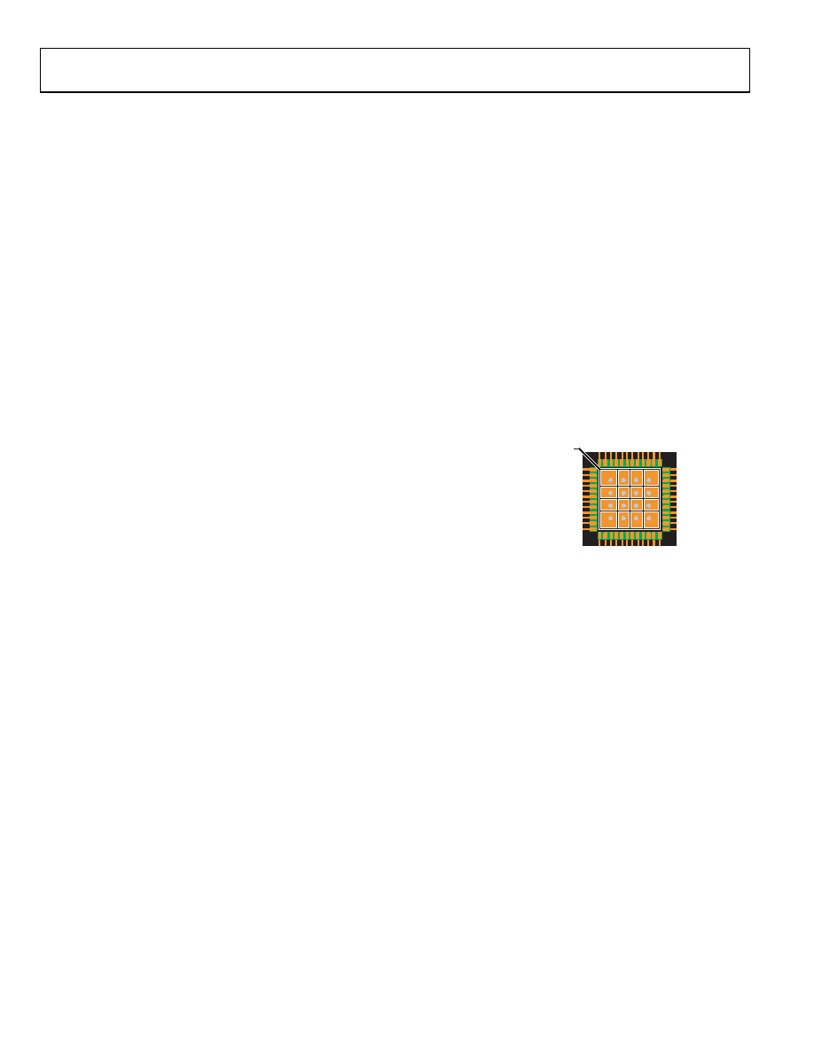
SILKSCREEN PARTITION
PIN 1 INDICATOR
05
72
6-
01
3
Figure 70. Typical PCB Layout
相关PDF资料 |
PDF描述 |
|---|---|
| MS3101A12S-3S | CONN RCPT 2POS FREE HNG W/SCKT |
| AD7686CRMZ | IC ADC 16BIT 500KSPS 10MSOP |
| VI-J41-MW-F2 | CONVERTER MOD DC/DC 12V 100W |
| AD7864ASZ-2 | IC ADC 12BIT PAR 520K 4CH 44MQFP |
| PT06A-14-15S | CONN PLUG 15POS W/SOCKETS SOLDER |
相关代理商/技术参数 |
参数描述 |
|---|---|
| AD9219ABCPZ-65 | 功能描述:IC ADC 10BIT SRL 65MSPS 64LFCSP RoHS:是 类别:集成电路 (IC) >> 数据采集 - 模数转换器 系列:- 其它有关文件:TSA1204 View All Specifications 标准包装:1 系列:- 位数:12 采样率(每秒):20M 数据接口:并联 转换器数目:2 功率耗散(最大):155mW 电压电源:模拟和数字 工作温度:-40°C ~ 85°C 安装类型:表面贴装 封装/外壳:48-TQFP 供应商设备封装:48-TQFP(7x7) 包装:Digi-Reel® 输入数目和类型:4 个单端,单极;2 个差分,单极 产品目录页面:1156 (CN2011-ZH PDF) 其它名称:497-5435-6 |
| AD9219ABCPZRL7-40 | 功能描述:IC ADC 10BIT SRL 40MSPS 64LFCSP RoHS:是 类别:集成电路 (IC) >> 数据采集 - 模数转换器 系列:- 标准包装:1,000 系列:- 位数:12 采样率(每秒):300k 数据接口:并联 转换器数目:1 功率耗散(最大):75mW 电压电源:单电源 工作温度:0°C ~ 70°C 安装类型:表面贴装 封装/外壳:24-SOIC(0.295",7.50mm 宽) 供应商设备封装:24-SOIC 包装:带卷 (TR) 输入数目和类型:1 个单端,单极;1 个单端,双极 |
| AD9219ABCPZRL7-65 | 功能描述:IC ADC 10BIT SRL 65MSPS 64LFCSP RoHS:是 类别:集成电路 (IC) >> 数据采集 - 模数转换器 系列:- 标准包装:1,000 系列:- 位数:12 采样率(每秒):300k 数据接口:并联 转换器数目:1 功率耗散(最大):75mW 电压电源:单电源 工作温度:0°C ~ 70°C 安装类型:表面贴装 封装/外壳:24-SOIC(0.295",7.50mm 宽) 供应商设备封装:24-SOIC 包装:带卷 (TR) 输入数目和类型:1 个单端,单极;1 个单端,双极 |
| AD9219BCPZ-40 | 制造商:Analog Devices 功能描述:ADC Quad Pipelined 40Msps 10-bit Serial 48-Pin LFCSP EP 制造商:Analog Devices 功能描述:IC 10BIT ADC QUAD 40MSPS LFCSP48 |
| AD9219BCPZ-65 | 制造商:Analog Devices 功能描述:ADC Quad Pipelined 65Msps 10-bit Serial 48-Pin LFCSP EP 制造商:Analog Devices 功能描述:IC 10BIT ADC QUAD 65MSPS LFCSP48 |
发布紧急采购,3分钟左右您将得到回复。