- 您现在的位置:买卖IC网 > PDF目录10512 > AD9222ABCPZ-65 (Analog Devices Inc)IC ADC 12BIT SRL 65MSPS 64LFCSP PDF资料下载
参数资料
| 型号: | AD9222ABCPZ-65 |
| 厂商: | Analog Devices Inc |
| 文件页数: | 17/60页 |
| 文件大小: | 0K |
| 描述: | IC ADC 12BIT SRL 65MSPS 64LFCSP |
| 标准包装: | 1 |
| 位数: | 12 |
| 采样率(每秒): | 65M |
| 数据接口: | 串行,SPI? |
| 转换器数目: | 8 |
| 功率耗散(最大): | 950.5mW |
| 电压电源: | 模拟和数字 |
| 工作温度: | -40°C ~ 85°C |
| 安装类型: | 表面贴装 |
| 封装/外壳: | 64-VFQFN 裸露焊盘,CSP |
| 供应商设备封装: | 64-LFCSP-VQ(9x9) |
| 包装: | 托盘 |
| 输入数目和类型: | 16 个单端,单极;8 个差分,单极 |
第1页第2页第3页第4页第5页第6页第7页第8页第9页第10页第11页第12页第13页第14页第15页第16页当前第17页第18页第19页第20页第21页第22页第23页第24页第25页第26页第27页第28页第29页第30页第31页第32页第33页第34页第35页第36页第37页第38页第39页第40页第41页第42页第43页第44页第45页第46页第47页第48页第49页第50页第51页第52页第53页第54页第55页第56页第57页第58页第59页第60页
AD9222
Data Sheet
Rev. F | Page 24 of 60
CLOCK INPUT CONSIDERATIONS
For optimum performance, the AD9222 sample clock inputs
(CLK+ and CLK) should be clocked with a differential signal.
This signal is typically ac-coupled to the CLK+ and CLK pins
via a transformer or capacitors. These pins are biased internally
and require no additional biasing.
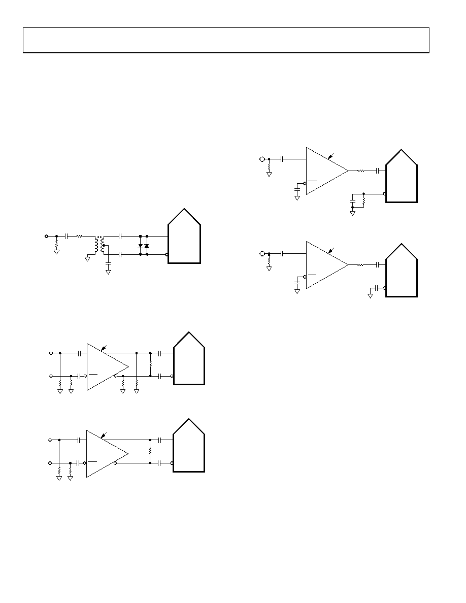
Figure 63 shows a preferred method for clocking the AD9222. The
low jitter clock source is converted from a single-ended signal
to a differential signal using an RF transformer. The back-to-
back Schottky diodes across the secondary transformer limit
clock excursions into the AD9222 to approximately 0.8 V p-p
differential. This helps prevent the large voltage swings of the
clock from feeding through to other portions of the AD9222,
and it preserves the fast rise and fall times of the signal, which
are critical to low jitter performance.
0.1F
SCHOTTKY
DIODES:
HSM2812
CLK+
50
100
CLK–
CLK+
ADC
AD9222
MINI-CIRCUITS
ADT1-1WT, 1:1Z
XFMR
05967-
050
Figure 63. Transformer-Coupled Differential Clock
Another option is to ac-couple a differential PECL signal to the
sample clock input pins as shown in Figure 64. The AD9510/
drivers offers excellent jitter performance.
CLK+
100
0.1F
240
240
CLK–
AD9510/AD9511/
AD9512/AD9513/
AD9514/AD9515
50
1
50
1
CLK
150
RESISTORS ARE OPTIONAL.
CLK–
CLK+
ADC
AD9222
05967-
051
PECL DRIVER
Figure 64. Differential PECL Sample Clock
CLK+
CLK–
10
0
0.1F
501
LVDS DRIVER
501
CLK
1
50 RESISTORS ARE OPTIONAL.
CLK–
CLK+
ADC
AD9222
05967-
052
AD9510/AD9511/
AD9512/AD9513/
AD9514/AD9515
Figure 65. Differential LVDS Sample Clock
In some applications, it is acceptable to drive the sample clock
inputs with a single-ended CMOS signal. In such applications,
CLK+ should be directly driven from a CMOS gate, and the
CLK pin should be bypassed to ground with a 0.1 μF capacitor
in parallel with a 39 k resistor (see Figure 66). Although the
CLK+ input circuit supply is AVDD (1.8 V), this input is
designed to withstand input voltages of up to 3.3 V, making the
selection of the drive logic voltage very flexible.
CLK+
0.1F
39k
CMOS DRIVER
50
1
OPTIONAL
100
0.1F
CLK
1
50 RESISTOR IS OPTIONAL.
CLK–
CLK+
ADC
AD9222
05967-
053
AD9510/AD9511/
AD9512/AD9513/
AD9514/AD9515
Figure 66. Single-Ended 1.8 V CMOS Sample Clock
CLK+
0.1F
CMOS DRIVER
50
1
OPTIONAL
100
CLK
150
RESISTOR IS OPTIONAL.
0.1F
CLK–
CLK+
ADC
AD9222
05967-
054
AD9510/AD9511/
AD9512/AD9513/
AD9514/AD9515
Figure 67. Single-Ended 3.3 V CMOS Sample Clock
Clock Duty Cycle Considerations
Typical high speed ADCs use both clock edges to generate a
variety of internal timing signals. As a result, these ADCs may
be sensitive to clock duty cycle. Commonly, a 5% tolerance is
required on the clock duty cycle to maintain dynamic performance
characteristics. The AD9222 contains a duty cycle stabilizer (DCS)
that retimes the nonsampling edge, providing an internal clock
signal with a nominal 50% duty cycle. This allows a wide range
of clock input duty cycles without affecting the performance of
the AD9222. When the DCS is on, noise and distortion perfor-
mance are nearly flat for a wide range of duty cycles. However,
some applications may require the DCS function to be off. If so,
keep in mind that the dynamic range performance can be affected
when operated in this mode. See the Memory Map section for
more details on using this feature.
The duty cycle stabilizer uses a delay-locked loop (DLL) to
create the nonsampling edge. As a result, any changes to the
sampling frequency require approximately eight clock cycles
to allow the DLL to acquire and lock to the new rate.
相关PDF资料 |
PDF描述 |
|---|---|
| MS3102E28-3S | CONN RCPT 3POS BOX MNT W/SCKT |
| LTC2220CUP-1#PBF | IC ADC 12BIT 185MSPS 64-QFN |
| MS3102E32-17PX | CONN RCPT 4POS BOX MNT W/PINS |
| UP050CH120J-B-B | CAP CER 12PF 50V 5% AXIAL |
| VE-BTY-MV | CONVERTER MOD DC/DC 3.3V 99W |
相关代理商/技术参数 |
参数描述 |
|---|---|
| AD9222ABCPZRL7-40 | 制造商:Analog Devices 功能描述:ADC OCTAL PIPELINED 40MSPS 12-BIT SERL 64LFCSP EP - Tape and Reel |
| AD9222ABCPZRL7-50 | 功能描述:IC ADC 12BIT SRL 50MSPS 64LFCSP RoHS:是 类别:集成电路 (IC) >> 数据采集 - 模数转换器 系列:- 标准包装:1 系列:- 位数:14 采样率(每秒):83k 数据接口:串行,并联 转换器数目:1 功率耗散(最大):95mW 电压电源:双 ± 工作温度:0°C ~ 70°C 安装类型:通孔 封装/外壳:28-DIP(0.600",15.24mm) 供应商设备封装:28-PDIP 包装:管件 输入数目和类型:1 个单端,双极 |
| AD9222ABCPZRL7-65 | 功能描述:IC ADC 12BIT SRL 65MSPS 64LFCSP RoHS:是 类别:集成电路 (IC) >> 数据采集 - 模数转换器 系列:- 标准包装:1 系列:- 位数:14 采样率(每秒):83k 数据接口:串行,并联 转换器数目:1 功率耗散(最大):95mW 电压电源:双 ± 工作温度:0°C ~ 70°C 安装类型:通孔 封装/外壳:28-DIP(0.600",15.24mm) 供应商设备封装:28-PDIP 包装:管件 输入数目和类型:1 个单端,双极 |
| AD9222BCPZ-40 | 制造商:Analog Devices 功能描述:Octal ADC Pipelined 40Msps 12-bit Serial 64-Pin LFCSP EP 制造商:Rochester Electronics LLC 功能描述: |
| AD9222BCPZ-50 | 制造商:Analog Devices 功能描述:ADC Octal Pipelined 50Msps 12-bit Serial 64-Pin LFCSP EP 制造商:Rochester Electronics LLC 功能描述:- Bulk 制造商:Analog Devices 功能描述:12BIT ADC OCTAL 50MSPS LFCSP-64 |
发布紧急采购,3分钟左右您将得到回复。