- 您现在的位置:买卖IC网 > PDF目录10512 > AD9222ABCPZ-65 (Analog Devices Inc)IC ADC 12BIT SRL 65MSPS 64LFCSP PDF资料下载
参数资料
| 型号: | AD9222ABCPZ-65 |
| 厂商: | Analog Devices Inc |
| 文件页数: | 36/60页 |
| 文件大小: | 0K |
| 描述: | IC ADC 12BIT SRL 65MSPS 64LFCSP |
| 标准包装: | 1 |
| 位数: | 12 |
| 采样率(每秒): | 65M |
| 数据接口: | 串行,SPI? |
| 转换器数目: | 8 |
| 功率耗散(最大): | 950.5mW |
| 电压电源: | 模拟和数字 |
| 工作温度: | -40°C ~ 85°C |
| 安装类型: | 表面贴装 |
| 封装/外壳: | 64-VFQFN 裸露焊盘,CSP |
| 供应商设备封装: | 64-LFCSP-VQ(9x9) |
| 包装: | 托盘 |
| 输入数目和类型: | 16 个单端,单极;8 个差分,单极 |
第1页第2页第3页第4页第5页第6页第7页第8页第9页第10页第11页第12页第13页第14页第15页第16页第17页第18页第19页第20页第21页第22页第23页第24页第25页第26页第27页第28页第29页第30页第31页第32页第33页第34页第35页当前第36页第37页第38页第39页第40页第41页第42页第43页第44页第45页第46页第47页第48页第49页第50页第51页第52页第53页第54页第55页第56页第57页第58页第59页第60页
Data Sheet
AD9222
Rev. F | Page 41 of 60
DEFAULT OPERATION AND JUMPER SELECTION
SETTINGS
The following is a list of the default and optional settings or
modes allowed on the AD9222 Rev. A evaluation board.
POWER: Connect the switching power supply that is
provided with the evaluation kit between a rated 100 V ac
to 240 V ac wall outlet at 47 Hz to 63 Hz and P701.
AIN: The evaluation board is set up for a transformer-
coupled analog input with an optimum 50 impedance
match of 150 MHz of bandwidth (see Figure 87). For more
bandwidth response, the differential capacitor across the
analog inputs can be changed or removed. The common
mode of the analog inputs is developed from the center
tap of the transformer or AVDD_DUT/2.
0
A
MPL
IT
U
D
E
(d
B
F
S)
FREQUENCY (MHz)
0
–18
–16
–14
–12
–10
–8
–6
–4
–2
50
100
150
200
250
300
350
400
450
500
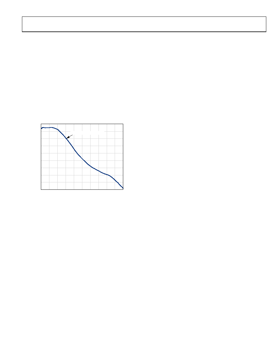
–3dB CUTOFF = 150MHz
05967-
071
Figure 87. Evaluation Board Full-Power Bandwidth, AD9222-50
VREF: VREF is set to 1.0 V by tying the SENSE pin to ground,
R317. This causes the ADC to operate in 2.0 V p-p full-scale
range. A separate external reference option using the ADR510
or ADR520 is also included on the evaluation board. Populate
R312 and R313 and remove C307. Proper use of the VREF
options is noted in the Voltage Reference section.
RBIAS: RBIAS has a default setting of 10 k (R301) to
ground and is used to set the ADC core bias current.
CLOCK: The default clock input circuitry is derived from a
simple transformer-coupled circuit using a high bandwidth
1:1 impedance ratio transformer (T401) that adds a very
low amount of jitter to the clock path. The clock input is
50 terminated and ac-coupled to handle single-ended
sine wave types of inputs. The transformer converts the
single-ended input to a differential signal that is clipped
before entering the ADC clock inputs.
A differential LVPECL clock can also be used to clock the
ADC input using the AD9515 (U401). Populate R406 and
R407 with 0 resistors and remove R215 and R216 to
disconnect the default clock path inputs. In addition, populate
C205 and C206 with a 0.1 μF capacitor and remove C409 and
C410 to disconnect the default clock path outputs. The
AD9515 has many pin-strappable options that are set to a
default mode of operation. Consult the AD9515 data sheet
for more information about these and other options.
In addition, an on-board oscillator is available on the OSC401
and can act as the primary clock source. The setup is quick
and involves installing R403 with a 0 resistor and setting
the enable jumper (J401) to the on position. If the user wishes
to employ a different oscillator, two oscillator footprint options
are available (OSC401) to check the ADC performance.
PDWN: To enable the power-down feature, short J301 to
the on position (AVDD) on the PDWN pin.
SCLK/DTP: To enable the digital test pattern on the digital
outputs of the ADC, use J304. If J304 is tied to AVDD during
device power-up, Test Pattern 1000 0000 0000 is enabled. See
the SCLK/DTP Pin section for details.
SDIO/ODM: To enable the low power, reduced signal option
(similar to the IEEE 1595.3 reduced range link LVDS output
standard), use J303. If J303 is tied to AVDD during device
power-up, it enables the LVDS outputs in a low power,
reduced signal option from the default ANSI-644 standard.
This option changes the signal swing from 350 mV p-p to
200 mV p-p, reducing the power of the DRVDD supply. See
the SDIO/ODM Pin section for more details.
CSB: To enable processing of the SPI information on the
SDIO and SCLK pins, tie J302 low in the always enable mode.
To ignore the SDIO and SCLK information, tie J302 to AVDD.
Non-SPI Mode: For users who wish to operate the DUT
without using SPI, remove Jumpers J302, J303, and J304.
This disconnects the CSB, SCLK/DTP, and SDIO/ODM pins
from the control bus, allowing the DUT to operate in its
simplest mode. Each of these pins has internal termination
and will float to its respective level.
D + x, D x: If an alternative data capture method to the setup
shown in Figure 90 is used, optional receiver terminations,
R318 and R320 to R328, can be installed next to the high
speed backplane connector.
相关PDF资料 |
PDF描述 |
|---|---|
| MS3102E28-3S | CONN RCPT 3POS BOX MNT W/SCKT |
| LTC2220CUP-1#PBF | IC ADC 12BIT 185MSPS 64-QFN |
| MS3102E32-17PX | CONN RCPT 4POS BOX MNT W/PINS |
| UP050CH120J-B-B | CAP CER 12PF 50V 5% AXIAL |
| VE-BTY-MV | CONVERTER MOD DC/DC 3.3V 99W |
相关代理商/技术参数 |
参数描述 |
|---|---|
| AD9222ABCPZRL7-40 | 制造商:Analog Devices 功能描述:ADC OCTAL PIPELINED 40MSPS 12-BIT SERL 64LFCSP EP - Tape and Reel |
| AD9222ABCPZRL7-50 | 功能描述:IC ADC 12BIT SRL 50MSPS 64LFCSP RoHS:是 类别:集成电路 (IC) >> 数据采集 - 模数转换器 系列:- 标准包装:1 系列:- 位数:14 采样率(每秒):83k 数据接口:串行,并联 转换器数目:1 功率耗散(最大):95mW 电压电源:双 ± 工作温度:0°C ~ 70°C 安装类型:通孔 封装/外壳:28-DIP(0.600",15.24mm) 供应商设备封装:28-PDIP 包装:管件 输入数目和类型:1 个单端,双极 |
| AD9222ABCPZRL7-65 | 功能描述:IC ADC 12BIT SRL 65MSPS 64LFCSP RoHS:是 类别:集成电路 (IC) >> 数据采集 - 模数转换器 系列:- 标准包装:1 系列:- 位数:14 采样率(每秒):83k 数据接口:串行,并联 转换器数目:1 功率耗散(最大):95mW 电压电源:双 ± 工作温度:0°C ~ 70°C 安装类型:通孔 封装/外壳:28-DIP(0.600",15.24mm) 供应商设备封装:28-PDIP 包装:管件 输入数目和类型:1 个单端,双极 |
| AD9222BCPZ-40 | 制造商:Analog Devices 功能描述:Octal ADC Pipelined 40Msps 12-bit Serial 64-Pin LFCSP EP 制造商:Rochester Electronics LLC 功能描述: |
| AD9222BCPZ-50 | 制造商:Analog Devices 功能描述:ADC Octal Pipelined 50Msps 12-bit Serial 64-Pin LFCSP EP 制造商:Rochester Electronics LLC 功能描述:- Bulk 制造商:Analog Devices 功能描述:12BIT ADC OCTAL 50MSPS LFCSP-64 |
发布紧急采购,3分钟左右您将得到回复。