- 您现在的位置:买卖IC网 > PDF目录10245 > AD9223ARSZ-REEL (Analog Devices Inc)IC ADC 12BIT 3.0MSPS 28SSOP PDF资料下载
参数资料
| 型号: | AD9223ARSZ-REEL |
| 厂商: | Analog Devices Inc |
| 文件页数: | 13/32页 |
| 文件大小: | 0K |
| 描述: | IC ADC 12BIT 3.0MSPS 28SSOP |
| 标准包装: | 1,500 |
| 位数: | 12 |
| 采样率(每秒): | 3M |
| 数据接口: | 并联 |
| 转换器数目: | 7 |
| 功率耗散(最大): | 130mW |
| 电压电源: | 单电源 |
| 工作温度: | -40°C ~ 85°C |
| 安装类型: | 表面贴装 |
| 封装/外壳: | 28-SSOP(0.209",5.30mm 宽) |
| 供应商设备封装: | 28-SSOP |
| 包装: | 带卷 (TR) |
| 输入数目和类型: | 2 个单端,单极;1 个差分,单极 |
第1页第2页第3页第4页第5页第6页第7页第8页第9页第10页第11页第12页当前第13页第14页第15页第16页第17页第18页第19页第20页第21页第22页第23页第24页第25页第26页第27页第28页第29页第30页第31页第32页
REV. E
–20–
AD9221/AD9223/AD9220
The AD9221/AD9223/AD9220 contains an internal reference
buffer, A2 (see Figure 9), that simplifies the drive requirements
of an external reference. The external reference must be able to
drive a
≈5 k (±20%) load. Note that the bandwidth of the
reference buffer is deliberately left small to minimize the refer-
ence noise contribution. As a result, it is not possible to change
the reference voltage rapidly in this mode without the removal
of the CAPT/CAPB Decoupling Network.
Variable Input Span with VCM = 2.5 V
Figure 24 shows an example of the AD9221/AD9223/AD9220
configured for an input span of 2
× VREF centered at 2.5 V. An
external 2.5 V reference drives the VINB pin, thus setting the
common-mode voltage at 2.5 V. The input span can be inde-
pendently set by a voltage divider consisting of R1 and R2,
which generates the VREF signal. A1 buffers this resistor net-
work and drives VREF. Choose this op amp based on accuracy
requirements. It is essential that a minimum of a 10
F capaci-
tor in parallel with a 0.1
F low inductance ceramic capacitor
decouple the reference output to ground.
2.5V+VREF
2.5V–VREF
2.5V
+5V
0.1 F
22 F
VINA
VINB
VREF
SENSE
+5V
R2
0.1 F
A1
R1
0.1 F
2.5V
REF
AD9221/
AD9223/
AD9220
Figure 24. External Reference—VCM = 2.5 V (2.5 V
on VINB, Resistor Divider to Make VREF)
Single-Ended Input with 0 to 2
VREF Range
Figure 25 shows an example of an external reference driving
both VINB and VREF. In this case, both the common-mode
voltage and input span are directly dependent on the value of
VREF. More specifically, the common-mode voltage is equal to
VREF while the input span is equal to 2
× VREF. Thus, the
valid input range extends from 0 to 2
× VREF. For example, if
the REF-191, a 2.048 external reference was selected, the valid
input range extends from 0 to 4.096 V. In this case, 1 LSB of
the AD9221/AD9223/AD9220 corresponds to 1 mV. It is essen-
tial that a minimum of a 10
F capacitor in parallel with a 0.1 F
low inductance ceramic capacitor decouple the reference output
to ground.
2 REF
0V
+5V
10 F
VINA
VINB
VREF
SENSE
AD9221/
AD9223/
AD9220
+5V
0.1 F
VREF
0.1 F
Figure 25. Input Range = 0 V to 2
× VREF
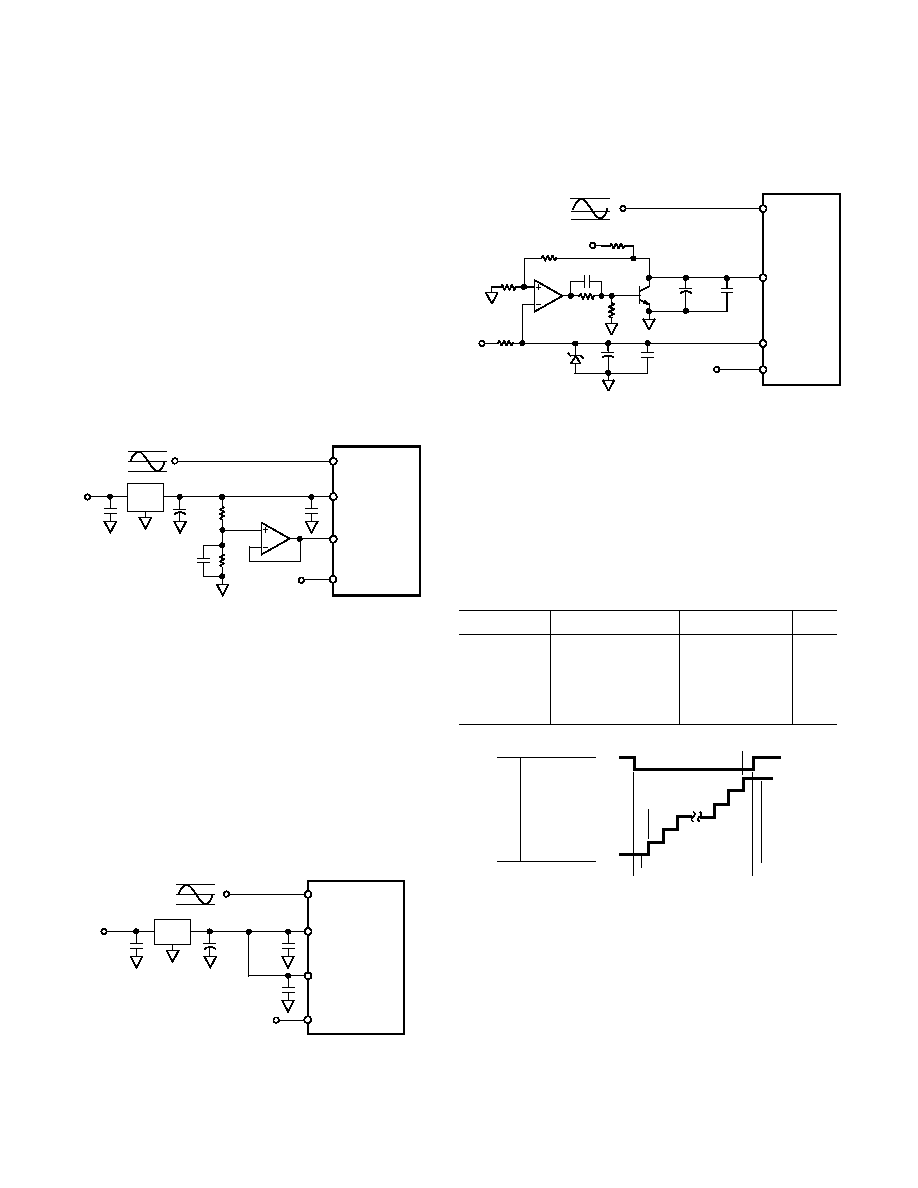
Low Cost/Power Reference
The external reference circuit shown in Figure 26 uses a low
cost 1.225 V external reference (e.g., AD580 or AD1580) along
with an op amp and transistor. The 2N2222 transistor acts in
conjunction with 1/2 of an OP282 to provide a very low imped-
ance drive for VINB. The selected op amp need not be a high
speed op amp and may be selected based on cost, power, and
accuracy.
3.75V
1.25V
5V
10 F
VINA
VINB
VREF
SENSE
AD9221/
AD9223/
AD9220
5V
0.1 F
316
1k
0.1 F
1/2
OP282
10 F
0.1 F
7.5k
AD1580
1k
820
5V
2N2222
1.225V
Figure 26. External Reference Using the AD1580
and Low Impedance Buffer
DIGITAL INPUTS AND OUTPUTS
Digital Outputs
The AD9221/AD9223/AD9220 output data is presented in
positive true straight binary for all input ranges. Table IV indi-
cates the output data formats for various input ranges regardless
of the selected input range. A twos complement output data
format can be created by inverting the MSB.
Table IV. Output Data Format
Input (V)
Condition (V)
Digital Output
OTR
VINA –VINB
< – VREF
0000 0000 0000
1
VINA –VINB
= – VREF
0000 0000 0000
0
VINA –VINB
= 0
1000 0000 0000
0
VINA –VINB
= + VREF – 1 LSB
1111 1111 1111
0
VINA –VINB
≥ + VREF
1111 1111 1111
1
1111 1111 1111
1111 1111 1110
OTR
–FS
+FS
–FS+1/2 LSB
+FS –1/2 LSB
–FS –1/2 LSB
+FS –1 1/2 LSB
0000 0000 0001
0000 0000 0000
1
0
1
OTR DATA OUTPUTS
Figure 27. Output Data Format
Out Of Range (OTR)
An out-of-range condition exists when the analog input voltage
is beyond the input range of the converter. OTR is a digital
output that is updated along with the data output corresponding
to the particular sampled analog input voltage. Thus, OTR has
the same pipeline delay (latency) as the digital data. It is LOW
when the analog input voltage is within the analog input range.
It is HIGH when the analog input voltage exceeds the input
range as shown in Figure 27. OTR will remain HIGH until the
analog input returns within the input range and another conver-
sion is completed. By logical ANDing OTR with the MSB and
its complement, overrange high or underrange low conditions
相关PDF资料 |
PDF描述 |
|---|---|
| AD9221ARSZ-REEL | IC ADC 12BIT 1.5MSPS 28SSOP |
| MS3106E22-22P | CONN PLUG 4POS STRAIGHT W/PINS |
| LTC1418IG#TRPBF | IC A/D CONV 14BIT SRL&PAR 28SSOP |
| D38999/20WD5PA | CONN RCPT 5POS WALL MNT W/PINS |
| MS3106E22-6S | CONN PLUG 3POS STRAIGHT W/SCKT |
相关代理商/技术参数 |
参数描述 |
|---|---|
| AD9223ARZ | 功能描述:IC ADC 12BIT 3.0MSPS 28SOIC RoHS:是 类别:集成电路 (IC) >> 数据采集 - 模数转换器 系列:- 其它有关文件:TSA1204 View All Specifications 标准包装:1 系列:- 位数:12 采样率(每秒):20M 数据接口:并联 转换器数目:2 功率耗散(最大):155mW 电压电源:模拟和数字 工作温度:-40°C ~ 85°C 安装类型:表面贴装 封装/外壳:48-TQFP 供应商设备封装:48-TQFP(7x7) 包装:Digi-Reel® 输入数目和类型:4 个单端,单极;2 个差分,单极 产品目录页面:1156 (CN2011-ZH PDF) 其它名称:497-5435-6 |
| AD9223ARZ-REEL | 功能描述:IC ADC 12BIT 3.0MSPS 28SOIC RoHS:是 类别:集成电路 (IC) >> 数据采集 - 模数转换器 系列:- 标准包装:1,000 系列:- 位数:12 采样率(每秒):300k 数据接口:并联 转换器数目:1 功率耗散(最大):75mW 电压电源:单电源 工作温度:0°C ~ 70°C 安装类型:表面贴装 封装/外壳:24-SOIC(0.295",7.50mm 宽) 供应商设备封装:24-SOIC 包装:带卷 (TR) 输入数目和类型:1 个单端,单极;1 个单端,双极 |
| AD9223-EB | 制造商:Analog Devices 功能描述:EVAL KIT FOR COMPLETE 12-BIT 1.5/3.0/10.0MSPS MONOLITHIC A/D - Bulk |
| AD9224 | 制造商:AD 制造商全称:Analog Devices 功能描述:Complete 12-Bit 40 MSPS Monolithic A/D Converter |
| AD9224ARS | 制造商:Analog Devices 功能描述:Analog/Digital Converter IC Number of Bi |
发布紧急采购,3分钟左右您将得到回复。