- 您现在的位置:买卖IC网 > PDF目录10245 > AD9223ARSZ-REEL (Analog Devices Inc)IC ADC 12BIT 3.0MSPS 28SSOP PDF资料下载
参数资料
| 型号: | AD9223ARSZ-REEL |
| 厂商: | Analog Devices Inc |
| 文件页数: | 32/32页 |
| 文件大小: | 0K |
| 描述: | IC ADC 12BIT 3.0MSPS 28SSOP |
| 标准包装: | 1,500 |
| 位数: | 12 |
| 采样率(每秒): | 3M |
| 数据接口: | 并联 |
| 转换器数目: | 7 |
| 功率耗散(最大): | 130mW |
| 电压电源: | 单电源 |
| 工作温度: | -40°C ~ 85°C |
| 安装类型: | 表面贴装 |
| 封装/外壳: | 28-SSOP(0.209",5.30mm 宽) |
| 供应商设备封装: | 28-SSOP |
| 包装: | 带卷 (TR) |
| 输入数目和类型: | 2 个单端,单极;1 个差分,单极 |
第1页第2页第3页第4页第5页第6页第7页第8页第9页第10页第11页第12页第13页第14页第15页第16页第17页第18页第19页第20页第21页第22页第23页第24页第25页第26页第27页第28页第29页第30页第31页当前第32页
REV. E
AD9221/AD9223/AD9220
–9–
INTRODUCTION
The AD9221/AD9223/AD9220 are members of a high perfor-
mance, complete single-supply 12-bit ADC product family based
on the same CMOS pipelined architecture. The product family
allows the system designer an upward or downward component
selection path based on dynamic performance, sample rate, and
power. The analog input range of the AD9221/AD9223/AD9220
is highly flexible, allowing for both single-ended or differen-
tial inputs of varying amplitudes that can be ac or dc coupled.
Each device shares the same interface options, pinout, and
package offering.
The AD9221/AD9223/AD9220 utilize a four-stage pipeline
architecture with a wideband input sample-and-hold amplifier
(SHA) implemented on a cost-effective CMOS process. Each
stage of the pipeline, excluding the last stage, consists of a low
resolution flash A/D connected to a switched capacitor DAC
and interstage residue amplifier (MDAC). The residue amplifier
amplifies the difference between the reconstructed DAC output
and the flash input for the next stage in the pipeline. One bit of
redundancy is used in each of the stages to facilitate digital
correction of flash errors. The last stage simply consists of a
flash A/D.
The pipeline architecture allows a greater throughput rate at the
expense of pipeline delay or latency. This means that while the
converter is capable of capturing a new input sample every clock
cycle, it actually takes three clock cycles for the conversion to be
fully processed and appear at the output. This latency is not a
concern in most applications. The digital output, together with
the out-of-range indicator (OTR), is latched into an output buffer
to drive the output pins. The output drivers can be configured to
interface with 5 V or 3.3 V logic families.
The AD9221/AD9223/AD9220 use both edges of the clock in
their internal timing circuitry (see Figure 1 and Specifications
for exact timing requirements). The A/D samples the analog
input on the rising edge of the clock input. During the clock low
time (between the falling edge and rising edge of the clock), the
input SHA is in the sample mode; during the clock high time, it
is in hold. System disturbances just prior to the rising edge of
the clock and/or excessive clock jitter may cause the input SHA
to acquire the wrong value, and should be minimized.
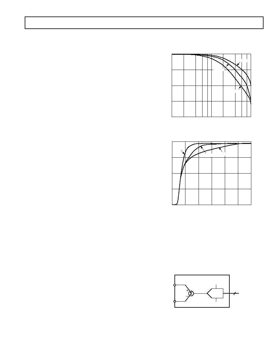
The internal circuitry of both the input SHA and individual
pipeline stages of each member of the product family are opti-
mized for both power dissipation and performance. An inherent
trade-off exists between the input SHA’s dynamic performance
and its power dissipation. Figures 2 and 3 show this trade-off by
comparing the full-power bandwidth and settling time of the
AD9221/AD9223/AD9220. Both figures reveal that higher full-
power bandwidths and faster settling times are achieved at the
expense of an increase in power dissipation. Similarly, a trade-
off exists between the sampling rate and the power dissipated
in each stage.
As previously stated, the AD9221, AD9223, and AD9220 are
similar in most aspects except for the specified sampling rate,
power consumption, and dynamic performance. The product
family is highly flexible, providing several different input ranges
and interface options. As a result, many of the application issues
and trade-offs associated with these resulting configurations are
also similar. The data sheet is structured such that the designer
can make an informed decision in selecting the proper A/D and
optimizing its performance to fit the specific application.
FREQUENCY – MHz
0
–3
–12
1
100
10
AMPLITUDE
–
dB
–6
–9
AD9221
AD9220
AD9223
Figure 2. Full-Power Bandwidth
SETTLING TIME – ns
CODE
4000
3000
0
60
10
20
30
40
50
2000
1000
AD9220
AD9223
AD9221
Figure 3. Settling Time
ANALOG INPUT AND REFERENCE OVERVIEW
Figure 4, a simplified model of the AD9221/AD9223/AD9220,
highlights the relationship between the analog inputs, VINA,
VINB, and the reference voltage, VREF. Like the voltage
applied to the top of the resistor ladder in a flash A/D converter,
the value VREF defines the maximum input voltage to the A/D
core. The minimum input voltage to the A/D core is automati-
cally defined to be –VREF.
VCORE
VINA
VINB
+VREF
–VREF
A/D
CORE
12
AD9221/AD9223/AD9220
Figure 4. AD9221/AD9223/AD9220 Equivalent
Functional Input Circuit
相关PDF资料 |
PDF描述 |
|---|---|
| AD9221ARSZ-REEL | IC ADC 12BIT 1.5MSPS 28SSOP |
| MS3106E22-22P | CONN PLUG 4POS STRAIGHT W/PINS |
| LTC1418IG#TRPBF | IC A/D CONV 14BIT SRL&PAR 28SSOP |
| D38999/20WD5PA | CONN RCPT 5POS WALL MNT W/PINS |
| MS3106E22-6S | CONN PLUG 3POS STRAIGHT W/SCKT |
相关代理商/技术参数 |
参数描述 |
|---|---|
| AD9223ARZ | 功能描述:IC ADC 12BIT 3.0MSPS 28SOIC RoHS:是 类别:集成电路 (IC) >> 数据采集 - 模数转换器 系列:- 其它有关文件:TSA1204 View All Specifications 标准包装:1 系列:- 位数:12 采样率(每秒):20M 数据接口:并联 转换器数目:2 功率耗散(最大):155mW 电压电源:模拟和数字 工作温度:-40°C ~ 85°C 安装类型:表面贴装 封装/外壳:48-TQFP 供应商设备封装:48-TQFP(7x7) 包装:Digi-Reel® 输入数目和类型:4 个单端,单极;2 个差分,单极 产品目录页面:1156 (CN2011-ZH PDF) 其它名称:497-5435-6 |
| AD9223ARZ-REEL | 功能描述:IC ADC 12BIT 3.0MSPS 28SOIC RoHS:是 类别:集成电路 (IC) >> 数据采集 - 模数转换器 系列:- 标准包装:1,000 系列:- 位数:12 采样率(每秒):300k 数据接口:并联 转换器数目:1 功率耗散(最大):75mW 电压电源:单电源 工作温度:0°C ~ 70°C 安装类型:表面贴装 封装/外壳:24-SOIC(0.295",7.50mm 宽) 供应商设备封装:24-SOIC 包装:带卷 (TR) 输入数目和类型:1 个单端,单极;1 个单端,双极 |
| AD9223-EB | 制造商:Analog Devices 功能描述:EVAL KIT FOR COMPLETE 12-BIT 1.5/3.0/10.0MSPS MONOLITHIC A/D - Bulk |
| AD9224 | 制造商:AD 制造商全称:Analog Devices 功能描述:Complete 12-Bit 40 MSPS Monolithic A/D Converter |
| AD9224ARS | 制造商:Analog Devices 功能描述:Analog/Digital Converter IC Number of Bi |
发布紧急采购,3分钟左右您将得到回复。