- 您现在的位置:买卖IC网 > PDF目录10245 > AD9223ARSZ-REEL (Analog Devices Inc)IC ADC 12BIT 3.0MSPS 28SSOP PDF资料下载
参数资料
| 型号: | AD9223ARSZ-REEL |
| 厂商: | Analog Devices Inc |
| 文件页数: | 7/32页 |
| 文件大小: | 0K |
| 描述: | IC ADC 12BIT 3.0MSPS 28SSOP |
| 标准包装: | 1,500 |
| 位数: | 12 |
| 采样率(每秒): | 3M |
| 数据接口: | 并联 |
| 转换器数目: | 7 |
| 功率耗散(最大): | 130mW |
| 电压电源: | 单电源 |
| 工作温度: | -40°C ~ 85°C |
| 安装类型: | 表面贴装 |
| 封装/外壳: | 28-SSOP(0.209",5.30mm 宽) |
| 供应商设备封装: | 28-SSOP |
| 包装: | 带卷 (TR) |
| 输入数目和类型: | 2 个单端,单极;1 个差分,单极 |
第1页第2页第3页第4页第5页第6页当前第7页第8页第9页第10页第11页第12页第13页第14页第15页第16页第17页第18页第19页第20页第21页第22页第23页第24页第25页第26页第27页第28页第29页第30页第31页第32页
REV. E
AD9221/AD9223/AD9220
–15–
AVDD
AD9221/
AD9223/
AD9220
RS1
30
VCC
VEE
OPTIONAL
AC COUPLING
CAPACITOR
D2
1N4148
D1
1N4148
RS2
20
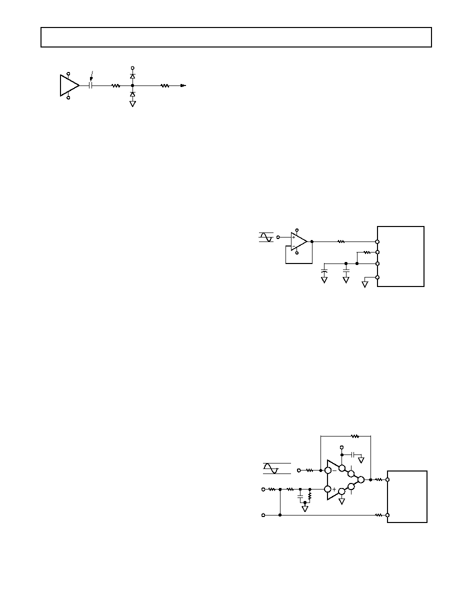
Figure 12. Simple Clamping Circuit
SINGLE-ENDED MODE OF OPERATION
The AD9221/AD9223/AD9220 can be configured for single-
ended operation using dc or ac coupling. In either case, the
input of the A/D must be driven from an operational amplifier
that will not degrade the A/D’s performance. Because the A/D
operates from a single-supply, it will be necessary to level-shift
ground-based bipolar signals to comply with its input require-
ments. Both dc and ac coupling provide this necessary function,
but each method results in different interface issues that may
influence the system design and performance.
DC COUPLING AND INTERFACE ISSUES
Many applications require the analog input signal to be dc-
coupled to the AD9221/AD9223/AD9220. An operational
amplifier can be configured to rescale and level shift the input
signal so that it is compatible with the selected input range of
the A/D. The input range to the A/D should be selected on the
basis of system performance objectives as well as the analog
power supply availability since this will place certain constraints
on the op amp selection.
Many of the new high performance op amps are specified for
only
±5 V operation and have limited input/output swing capa-
bilities. Therefore, the selected input range of the AD9221/
AD9223/AD9220 should be sensitive to the headroom require-
ments of the particular op amp to prevent clipping of the signal.
Also, since the output of a dual supply amplifier can swing
below –0.3 V, clamping its output should be considered in some
applications.
In some applications, it may be advantageous to use an op
amp specified for single-supply 5 V operation since it will
inherently limit its output swing to within the power supply
rails. An amplifier like the AD8041, AD8011, and AD817 are
useful for this purpose. Rail-to-rail output amplifiers such as
the AD8041 allow the AD9221/AD9223/AD9220 to be con-
figured for larger input spans, which improves the noise
performance.
If the application requires the largest input span (i.e., 0 V to
5 V) of the AD9221/AD9223/AD9220, the op amp will require
larger supplies to drive it. Various high speed amplifiers in the
Op Amp Selection Guide of this data sheet can be selected to
accommodate a wide range of supply options. Once again,
clamping the output of the amplifier should be considered for
these applications.
Two dc-coupled op amp circuits using a noninverting and
inverting topology are discussed below. Although not shown,
the noninverting and inverting topologies can be easily config-
ured as part of an antialiasing filter by using a Sallen-Key or
Multiple-Feedback topology, respectively. An additional R-C
network can be inserted between the op amp’s output and the
AD9221/AD9223/AD9220 input to provide a real pole.
Simple Op Amp Buffer
In the simplest case, the input signal to the AD9221/AD9223/
AD9220 will already be biased at levels in accordance with the
selected input range. It is simply necessary to provide an
adequately low source impedance for the VINA and VINB
analog input pins of the A/D. Figure 13 shows the recommended
configuration for a single-ended drive using an op amp. In this
case, the op amp is shown in a noninverting unity gain configu-
ration driving the VINA pin. The internal reference drives the
VINB pin. Note that the addition of a small series resistor of
30
to 50 connected to VINA and VINB will be beneficial
in nearly all cases. Refer to the Analog Input Operation section
for a discussion on resistor selection. Figure 13 shows the
proper connection for a 0 V to 5 V input range. Alternative
single-ended input ranges of 0 V to 2
× VREF can also be real-
ized with the proper configuration of VREF (refer to the Using
the Internal Reference section).
10 F
VINA
VINB
SENSE
AD9221/
AD9223/
AD9220
0.1 F
RS
+V
–V
RS
VREF
5V
0V
2.5V
U1
Figure 13. Single-Ended AD9221/AD9223/AD9220
Op Amp Drive Circuit
Op Amp with DC Level Shifting
Figure 14 shows a dc-coupled level shifting circuit employing an
op amp, A1, to sum the input signal with the desired dc offset.
Configuring the op amp in the inverting mode with the given
resistor values results in an ac signal gain of –1. If the signal
inversion is undesirable, interchange the VINA and VINB con-
nections to re-establish the original signal polarity. The dc voltage
at VREF sets the common-mode voltage of the AD9221/AD9223/
AD9220. For example, when VREF = 2.5 V, the output level
from the op amp will also be centered around 2.5 V. The use of
ratio matched, thin-film resistor networks will minimize gain
and offset errors. Also, an optional pull-up resistor, RP, may be
used to reduce the output load on VREF to
±1 mA.
0VDC
+VREF
–VREF
VINA
VINB
0.1 F
500 1
0.1 F
500 1
7
1
2
3
4
5
A1
6
NC
+VCC
500 1
RS
VREF
500 1
RS
RP
2
AVDD
NOTES
1OPTIONAL RESISTOR NETWORK-OHMTEK ORNA500D
2OPTIONAL PULL-UP RESISTOR WHEN USING INTERNAL REFERENCE
AD9221/
AD9223/
AD9220
Figure 14. Single-Ended Input with DC-Coupled
Level Shift
相关PDF资料 |
PDF描述 |
|---|---|
| AD9221ARSZ-REEL | IC ADC 12BIT 1.5MSPS 28SSOP |
| MS3106E22-22P | CONN PLUG 4POS STRAIGHT W/PINS |
| LTC1418IG#TRPBF | IC A/D CONV 14BIT SRL&PAR 28SSOP |
| D38999/20WD5PA | CONN RCPT 5POS WALL MNT W/PINS |
| MS3106E22-6S | CONN PLUG 3POS STRAIGHT W/SCKT |
相关代理商/技术参数 |
参数描述 |
|---|---|
| AD9223ARZ | 功能描述:IC ADC 12BIT 3.0MSPS 28SOIC RoHS:是 类别:集成电路 (IC) >> 数据采集 - 模数转换器 系列:- 其它有关文件:TSA1204 View All Specifications 标准包装:1 系列:- 位数:12 采样率(每秒):20M 数据接口:并联 转换器数目:2 功率耗散(最大):155mW 电压电源:模拟和数字 工作温度:-40°C ~ 85°C 安装类型:表面贴装 封装/外壳:48-TQFP 供应商设备封装:48-TQFP(7x7) 包装:Digi-Reel® 输入数目和类型:4 个单端,单极;2 个差分,单极 产品目录页面:1156 (CN2011-ZH PDF) 其它名称:497-5435-6 |
| AD9223ARZ-REEL | 功能描述:IC ADC 12BIT 3.0MSPS 28SOIC RoHS:是 类别:集成电路 (IC) >> 数据采集 - 模数转换器 系列:- 标准包装:1,000 系列:- 位数:12 采样率(每秒):300k 数据接口:并联 转换器数目:1 功率耗散(最大):75mW 电压电源:单电源 工作温度:0°C ~ 70°C 安装类型:表面贴装 封装/外壳:24-SOIC(0.295",7.50mm 宽) 供应商设备封装:24-SOIC 包装:带卷 (TR) 输入数目和类型:1 个单端,单极;1 个单端,双极 |
| AD9223-EB | 制造商:Analog Devices 功能描述:EVAL KIT FOR COMPLETE 12-BIT 1.5/3.0/10.0MSPS MONOLITHIC A/D - Bulk |
| AD9224 | 制造商:AD 制造商全称:Analog Devices 功能描述:Complete 12-Bit 40 MSPS Monolithic A/D Converter |
| AD9224ARS | 制造商:Analog Devices 功能描述:Analog/Digital Converter IC Number of Bi |
发布紧急采购,3分钟左右您将得到回复。