- 您现在的位置:买卖IC网 > PDF目录10245 > AD9223ARSZ-REEL (Analog Devices Inc)IC ADC 12BIT 3.0MSPS 28SSOP PDF资料下载
参数资料
| 型号: | AD9223ARSZ-REEL |
| 厂商: | Analog Devices Inc |
| 文件页数: | 14/32页 |
| 文件大小: | 0K |
| 描述: | IC ADC 12BIT 3.0MSPS 28SSOP |
| 标准包装: | 1,500 |
| 位数: | 12 |
| 采样率(每秒): | 3M |
| 数据接口: | 并联 |
| 转换器数目: | 7 |
| 功率耗散(最大): | 130mW |
| 电压电源: | 单电源 |
| 工作温度: | -40°C ~ 85°C |
| 安装类型: | 表面贴装 |
| 封装/外壳: | 28-SSOP(0.209",5.30mm 宽) |
| 供应商设备封装: | 28-SSOP |
| 包装: | 带卷 (TR) |
| 输入数目和类型: | 2 个单端,单极;1 个差分,单极 |
第1页第2页第3页第4页第5页第6页第7页第8页第9页第10页第11页第12页第13页当前第14页第15页第16页第17页第18页第19页第20页第21页第22页第23页第24页第25页第26页第27页第28页第29页第30页第31页第32页
REV. E
AD9221/AD9223/AD9220
–21–
can be detected. Table V is a truth table for the over/underrange
circuit in Figure 28, which uses NAND gates. Systems requiring
programmable gain conditioning of the AD9221/AD9223/
AD9220 input signal can immediately detect an out-of-range
condition, thus eliminating gain selection iterations. Also, OTR
can be used for digital offset and gain calibration.
Table V. Out-of-Range Truth Table
OTR
MSB
Analog Input Is
00
In Range
01
In Range
10
Underrange
11
Overrange
OVER = “1”
UNDER = “1”
MSB
OTR
MSB
Figure 28. Overrange or Underrange Logic
Digital Output Driver Considerations (DVDD)
The AD9221, AD9223 and AD9220 output drivers can be
configured to interface with 5 V or 3.3 V logic families by setting
DVDD to 5 V or 3.3 V respectively. The AD9221/AD9223/
AD9220 output drivers are sized to provide sufficient output
current to drive a wide variety of logic families. However, large
drive currents tend to cause glitches on the supplies and may
affect SINAD performance. Applications requiring the AD9221/
AD9223/AD9220 to drive large capacitive loads or large fanout
may require additional decoupling capacitors on DVDD. In
extreme cases, external buffers or latches may be required.
Clock Input and Considerations
The AD9221/AD9223/AD9220 internal timing uses the two
edges of the clock input to generate a variety of internal timing
signals. The clock input must meet or exceed the minimum
specified pulsewidth high and low (tCH and tCL) specifications
for the given A/D as defined in the Switching Specifications to
meet the rated performance specifications. For example, the
clock input to the AD9220 operating at 10 MSPS may have a
duty cycle between 45% to 55% to meet this timing requirement
since the minimum specified tCH and tCL is 45 ns. For clock
rates below 10 MSPS, the duty cycle may deviate from this
range to the extent that both tCH and tCL are satisfied.
All high speed high resolution A/Ds are sensitive to the quality
of the clock input. The degradation in SNR at a given full-scale
input frequency (fIN) due to only aperture jitter (tA) can be
calculated with the following equation:
SNR
f
t
IN
A
=
[]
20
1 2
10
log
/
π
In the equation, the rms aperture jitter, tA, represents the root-
sum square of all the jitter sources, which include the clock
input, analog input signal, and A/D aperture jitter specification.
For example, if a 5 MHz full-scale sine wave is sampled by an
A/D with a total rms jitter of 15 ps, the SNR performance of the
A/D will be limited to 66.5 dB. Undersampling applications are
particularly sensitive to jitter.
The clock input should be treated as an analog signal in cases
where aperture jitter may affect the dynamic range of the AD9221/
AD9223/AD9220. As such, supplies for clock drivers should be
separated from the A/D output driver supplies to avoid modulating
the clock signal with digital noise. Low jitter crystal controlled
oscillators make the best clock sources. If the clock is generated
from another type of source (by gating, dividing, or other method),
it should be retimed by the original clock at the last step.
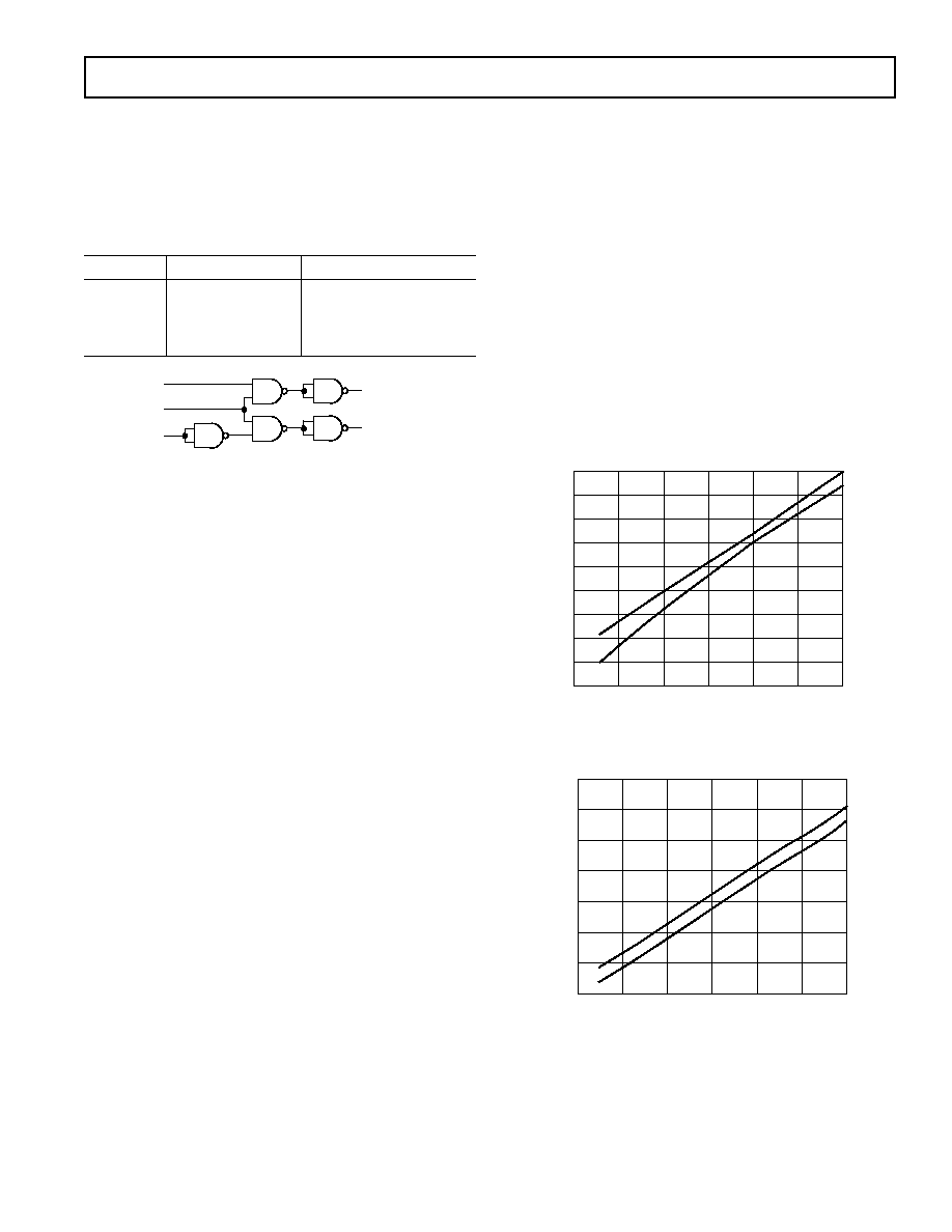
Most of the power dissipated by the AD9221/AD9223/AD9220
is from the analog power supplies. However, lower clock speeds
will reduce digital current slightly. Figure 29 shows the relation-
ship between power and clock rate for each A/D.
CLOCK FREQUENCY – MHz
66
64
56
3.0
POWER
–
mW
2.5
62
60
58
5V p-p
2V p-p
54
52
50
48
2.0
1.5
1.0
0.5
Figure 29a. AD9221 Power Consumption vs. Clock
Frequency
CLOCK FREQUENCY – MHz
125
120
105
6
POWER
–
mW
5
115
110
5V p-p
2V p-p
100
95
90
4
3
2
1
0
Figure 29b. AD9223 Power Consumption vs. Clock
Frequency
相关PDF资料 |
PDF描述 |
|---|---|
| AD9221ARSZ-REEL | IC ADC 12BIT 1.5MSPS 28SSOP |
| MS3106E22-22P | CONN PLUG 4POS STRAIGHT W/PINS |
| LTC1418IG#TRPBF | IC A/D CONV 14BIT SRL&PAR 28SSOP |
| D38999/20WD5PA | CONN RCPT 5POS WALL MNT W/PINS |
| MS3106E22-6S | CONN PLUG 3POS STRAIGHT W/SCKT |
相关代理商/技术参数 |
参数描述 |
|---|---|
| AD9223ARZ | 功能描述:IC ADC 12BIT 3.0MSPS 28SOIC RoHS:是 类别:集成电路 (IC) >> 数据采集 - 模数转换器 系列:- 其它有关文件:TSA1204 View All Specifications 标准包装:1 系列:- 位数:12 采样率(每秒):20M 数据接口:并联 转换器数目:2 功率耗散(最大):155mW 电压电源:模拟和数字 工作温度:-40°C ~ 85°C 安装类型:表面贴装 封装/外壳:48-TQFP 供应商设备封装:48-TQFP(7x7) 包装:Digi-Reel® 输入数目和类型:4 个单端,单极;2 个差分,单极 产品目录页面:1156 (CN2011-ZH PDF) 其它名称:497-5435-6 |
| AD9223ARZ-REEL | 功能描述:IC ADC 12BIT 3.0MSPS 28SOIC RoHS:是 类别:集成电路 (IC) >> 数据采集 - 模数转换器 系列:- 标准包装:1,000 系列:- 位数:12 采样率(每秒):300k 数据接口:并联 转换器数目:1 功率耗散(最大):75mW 电压电源:单电源 工作温度:0°C ~ 70°C 安装类型:表面贴装 封装/外壳:24-SOIC(0.295",7.50mm 宽) 供应商设备封装:24-SOIC 包装:带卷 (TR) 输入数目和类型:1 个单端,单极;1 个单端,双极 |
| AD9223-EB | 制造商:Analog Devices 功能描述:EVAL KIT FOR COMPLETE 12-BIT 1.5/3.0/10.0MSPS MONOLITHIC A/D - Bulk |
| AD9224 | 制造商:AD 制造商全称:Analog Devices 功能描述:Complete 12-Bit 40 MSPS Monolithic A/D Converter |
| AD9224ARS | 制造商:Analog Devices 功能描述:Analog/Digital Converter IC Number of Bi |
发布紧急采购,3分钟左右您将得到回复。