- 您现在的位置:买卖IC网 > PDF目录10664 > AD9243ASZ (Analog Devices Inc)IC ADC 14BIT 3MSPS 44-MQFP PDF资料下载
参数资料
| 型号: | AD9243ASZ |
| 厂商: | Analog Devices Inc |
| 文件页数: | 6/24页 |
| 文件大小: | 0K |
| 描述: | IC ADC 14BIT 3MSPS 44-MQFP |
| 标准包装: | 1 |
| 位数: | 14 |
| 采样率(每秒): | 3M |
| 数据接口: | 并联 |
| 转换器数目: | 7 |
| 功率耗散(最大): | 145mW |
| 电压电源: | 模拟和数字 |
| 工作温度: | -40°C ~ 85°C |
| 安装类型: | 表面贴装 |
| 封装/外壳: | 44-QFP |
| 供应商设备封装: | 44-MQFP(10x10) |
| 包装: | 托盘 |
| 输入数目和类型: | 2 个单端,单极;1 个差分,单极 |
AD9243
REV. A
–14–
If the application requires the largest single-ended input range
(i.e., 0 V to 5 V) of the AD9243, the op amp will require larger
supplies to drive it. Various high speed amplifiers in the “Op
Amp Selection Guide” of this data sheet can be selected to
accommodate a wide range of supply options. Once again,
clamping the output of the amplifier should be considered for
these applications. Alternatively, a single-ended to differential
op amp driver circuit using the AD8042 could be used to
achieve the 5 V input span while operating from a single +5 V
supply.
Two dc coupled op amp circuits using a noninverting and inverting
topology are discussed below. Although not shown, the nonin-
verting and inverting topologies can be easily configured as part
of an antialiasing filter by using a Sallen-Key or Multiple-Feed-
back topology, respectively. An additional R-C network can be
inserted between the op amp’s output and the AD9243 input to
provide a real pole.
Simple Op Amp Buffer
In the simplest case, the input signal to the AD9243 will already
be biased at levels in accordance with the selected input range.
It is simply necessary to provide an adequately low source im-
pedance for the VINA and VINB analog input pins of the A/D.
Figure 32 shows the recommended configuration for a single-
ended drive using an op amp. In this case, the op amp is shown
in a noninverting unity gain configuration driving the VINA pin.
The internal reference drives the VINB pin. Note that the
addition of a small series resistor of 30
to 50 connected to
VINA and VINB will be beneficial in nearly all cases. Refer to
section “Analog Input Operation” for a discussion on resistor
selection. Figure 32 shows the proper connection for a 0 V to 5 V
input range. Alternative single ended input ranges of 0 V to 2
×
VREF can also be realized with the proper configuration of VREF
(refer to the section “Using the Internal Reference”).
10 F
VINA
VINB
SENSE
AD9243
0.1 F
RS
+V
–V
RS
VREF
5V
0V
U1
2.5V
Figure 32. Single-Ended AD9243 Op Amp Drive Circuit
Op Amp with DC Level Shifting
Figure 33 shows a dc-coupled level shifting circuit employing an
op amp, A1, to sum the input signal with the desired dc offset.
Configuring the op amp in the inverting mode with the given
resistor values results in an ac signal gain of –1. If the signal
inversion is undesirable, interchange the VINA and VINB con-
nections to reestablish the original signal polarity. The dc volt-
age at VREF sets the common-mode voltage of the AD9243. For
example, when VREF = 2.5 V, the output level from the op amp
will also be centered around 2.5 V. The use of ratio matched,
thin-film resistor networks will minimize gain and offset errors.
Also, an optional pull-up resistor, RP, may be used to reduce the
output load on VREF to
±1 mA.
0VDC
+VREF
–VREF
VINA
VINB
AD9243
0.1 F
500 *
0.1 F
500 *
7
1
2
3
4
5
A1
6
NC
+VCC
500 *
RS
VREF
500 *
RS
AVDD
RP**
*OPTIONAL RESISTOR NETWORK-OHMTEK ORNA500D
**OPTIONAL PULL-UP RESISTOR WHEN USING INTERNAL REFERENCE
NC = NO CONNECT
Figure 33. Single-Ended Input With DC-Coupled Level Shift
AC COUPLING AND INTERFACE ISSUES
For applications where ac coupling is appropriate, the op amp’s
output can be easily level shifted to the common-mode voltage,
VCM, of the AD9243 via a coupling capacitor. This has the
advantage of allowing the op amps common-mode level to be
symmetrically biased to its midsupply level (i.e., (VCC + VEE)/2).
Op amps which operate symmetrically with respect to their
power supplies typically provide the best ac performance as well
as greatest input/output span. Hence, various high speed/perfor-
mance amplifiers which are restricted to +5 V/–5 V operation
and/or specified for +5 V single-supply operation can be easily
configured for the 5 V or 2 V input span of the AD9243, respec-
tively. The best ac distortion performance is achieved when the
A/D is configured for a 2 V input span and common-mode
voltage of 2.5 V. Note that differential transformer coupling,
which is another form of ac coupling, should be considered for
optimum ac performance.
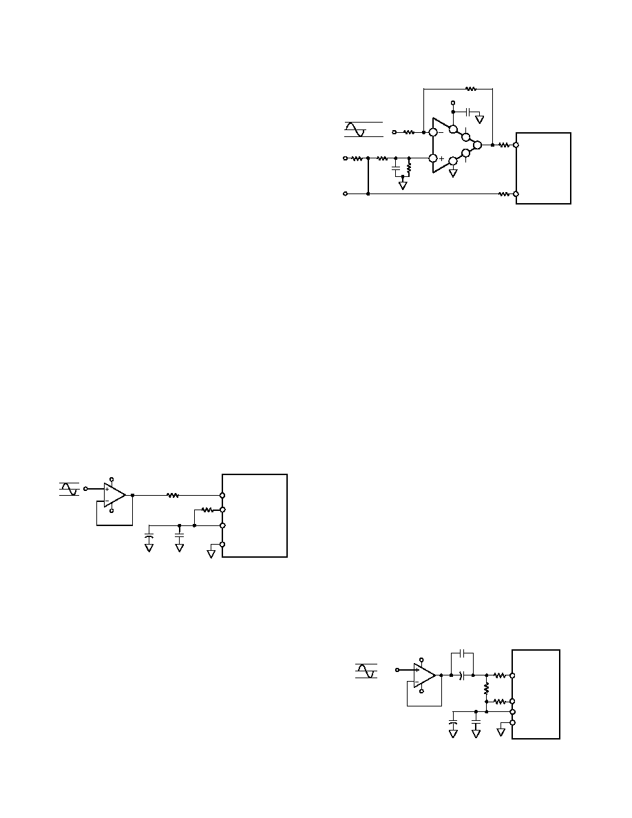
Simple AC Interface
Figure 34 shows a typical example of an ac-coupled, single-
ended configuration. The bias voltage shifts the bipolar, ground-
referenced input signal to approximately VREF. The value for
C1 and C2 will depend on the size of the resistor, R. The ca-
pacitors, C1 and C2, are typically a 0.1
F ceramic and 10 F
tantalum capacitor in parallel to achieve a low cutoff frequency
while maintaining a low impedance over a wide frequency range.
The combination of the capacitor and the resistor form a high-
pass filter with a high-pass –3 dB frequency determined by the
equation,
f–3 dB = 1/(2
× π × R × (C1 + C2))
The low impedance VREF voltage source biases both the VINB
input and provides the bias voltage for the VINA input. Figure
34 shows the VREF configured for 2.5 V. Thus the input range
C2
VINA
VINB
SENSE
AD9243
C1
R
+5V
–5V
RS
VREF
+VREF
0V
–VREF
VIN
C2
C1
RS
Figure 34. AC-Coupled Input
相关PDF资料 |
PDF描述 |
|---|---|
| AD7893ANZ-2 | IC ADC 12BIT SRL T/H LP 8-DIP |
| MAX9034AUD+T | IC COMPARATOR QUAD 14-TSSOP |
| MAX9039BEBT+T | IC COMPARATOR SNGL 6-UCSP |
| LTC1415CSW#PBF | IC A/D CONV 12BIT SAMPLNG 28SOIC |
| VE-B13-MX-F2 | CONVERTER MOD DC/DC 24V 75W |
相关代理商/技术参数 |
参数描述 |
|---|---|
| AD9243ASZRL | 功能描述:IC ADC 14BIT SGL 3MSPS 44MQFP RoHS:是 类别:集成电路 (IC) >> 数据采集 - 模数转换器 系列:- 标准包装:1,000 系列:- 位数:12 采样率(每秒):300k 数据接口:并联 转换器数目:1 功率耗散(最大):75mW 电压电源:单电源 工作温度:0°C ~ 70°C 安装类型:表面贴装 封装/外壳:24-SOIC(0.295",7.50mm 宽) 供应商设备封装:24-SOIC 包装:带卷 (TR) 输入数目和类型:1 个单端,单极;1 个单端,双极 |
| AD9243EB | 制造商:AD 制造商全称:Analog Devices 功能描述:Complete 14-Bit, 3.0 MSPS Monolithic A/D Converter |
| AD9243-EB | 制造商:Analog Devices 功能描述:Evaluation Board For AD9243 制造商:Analog Devices 功能描述:DEV TOOLS, EVAL BD FOR AD9243 - Bulk |
| AD9244 | 制造商:AD 制造商全称:Analog Devices 功能描述:14-Bit, 40/65 MSPS Monolithic A/D Converter |
| AD9244_05 | 制造商:AD 制造商全称:Analog Devices 功能描述:14-Bit, 40 MSPS/65 MSPS A/D Converter |
发布紧急采购,3分钟左右您将得到回复。