- 您现在的位置:买卖IC网 > PDF目录10664 > AD9243ASZ (Analog Devices Inc)IC ADC 14BIT 3MSPS 44-MQFP PDF资料下载
参数资料
| 型号: | AD9243ASZ |
| 厂商: | Analog Devices Inc |
| 文件页数: | 8/24页 |
| 文件大小: | 0K |
| 描述: | IC ADC 14BIT 3MSPS 44-MQFP |
| 标准包装: | 1 |
| 位数: | 14 |
| 采样率(每秒): | 3M |
| 数据接口: | 并联 |
| 转换器数目: | 7 |
| 功率耗散(最大): | 145mW |
| 电压电源: | 模拟和数字 |
| 工作温度: | -40°C ~ 85°C |
| 安装类型: | 表面贴装 |
| 封装/外壳: | 44-QFP |
| 供应商设备封装: | 44-MQFP(10x10) |
| 包装: | 托盘 |
| 输入数目和类型: | 2 个单端,单极;1 个差分,单极 |
AD9243
REV. A
–16–
Shorting the VREF pin directly to the SENSE pin places the
internal reference amplifier in unity-gain mode and the resultant
VREF output is 1 V. Therefore, the valid input range is 0 V to
2 V. However, shorting the SENSE pin directly to the REFCOM
pin configures the internal reference amplifier for a gain of 2.5
and the resultant VREF output is 2.5 V. Thus, the valid input
range becomes 0 V to 5 V. The VREF pin should be bypassed
to the REFCOM pin with a 10
F tantalum capacitor in parallel
with a low-inductance 0.1
F ceramic capacitor.
10 F
VINA
VREF
AD9243
0.1 F
VINB
2xVREF
0V
SHORT FOR 0V TO 2V
INPUT SPAN
SENSE
SHORT FOR 0V TO 5V
INPUT SPAN
REFCOM
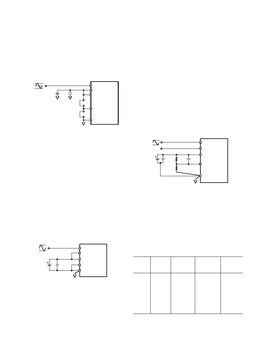
Figure 36. Internal Reference (2 V p-p Input Span,
VCM = 1 V, or 5 V p-p Input Span, VCM = 2.5 V)
Single-Ended or Differential Input, VCM = 2.5 V
Figure 37 shows the single-ended configuration that gives the
best SINAD performance. To optimize dynamic specifications,
center the common-mode voltage of the analog input at
approximately by 2.5 V by connecting VINB to VREF, a low-
impedance 2.5 V source. As described above, shorting the
SENSE pin directly to the REFCOM pin results in a 2.5 V
reference voltage and a 5 V p-p input span. The valid range
for input signals is 0 V to 5 V. The VREF pin should be by-
passed to the REFCOM pin with a 10
F tantalum capacitor in
parallel with a low inductance 0.1
F ceramic capacitor.
This reference configuration could also be used for a differential
input in which VINA and VINB are driven via a transformer as
shown in Figure 29. In this case, the common-mode voltage,
VCM, is set at midsupply by connecting the transformers center
tap to CML of the AD9243. VREF can be configured for 1 V
or 2.5 V by connecting SENSE to either VREF or REFCOM
respectively. Note that the valid input range for each of the
differential inputs is one half of the single-ended input and thus
becomes VCM – VREF/2 to VCM + VREF/2.
0.1 F
10 F
VINA
VINB
VREF
SENSE
REFCOM
AD9243
5V
0V
2.5V
Figure 37. Internal Reference—5 V p-p Input Span,
VCM = 2.5 V
Resistor Programmable Reference
Figure 38 shows an example of how to generate a reference
voltage other than 1 V or 2.5 V with the addition of two exter-
nal resistors and a bypass capacitor. Use the equation,
VREF = 1 V
× (1 + R1/R2),
to determine appropriate values for R1 and R2. These resistors
should be in the 2 k
to 100 k range. For the example shown,
R1 equals 2.5 k
and R2 equals 5 k. From the equation
above, the resultant reference voltage on the VREF pin is
1.5 V. This sets the input span to be 3 V p-p. To assure stabil-
ity, place a 0.1
F ceramic capacitor in parallel with R1.
The common-mode voltage can be set to VREF by connecting
VINB to VREF to provide an input span of 0 to 2
× VREF.
Alternatively, the common-mode voltage can be set to 2.5 V
by connecting VINB to a low impedance 2.5 V source. For
the example shown, the valid input single range for VINA is
1 V to 4 V since VINB is set to an external, low impedance 2.5
V source. The VREF pin should be bypassed to the REFCOM
pin with a 10
F tantalum capacitor in parallel with a low induc-
tance 0.1
F ceramic capacitor.
4V
1V
1.5V
C1
0.1 F
10 F
VINA
VINB
VREF
SENSE
REFCOM
AD9243
2.5V
R1
2.5k
R2
5k
0.1 F
Figure 38. Resistor Programmable Reference (3 V p-p
Input Span, VCM = 2.5 V)
USING AN EXTERNAL REFERENCE
Using an external reference may enhance the dc performance of
the AD9243 by improving drift and accuracy. Figures 39
through 41 show examples of how to use an external reference
with the A/D. Table III is a list of suitable voltage references
from Analog Devices. To use an external reference, the user
must disable the internal reference amplifier and drive the VREF
pin. Connecting the SENSE pin to AVDD disables the inter-
nal reference amplifier.
Table III. Suitable Voltage References
Initial
Operating
Output
Drift
Accuracy
Current
Voltage
(ppm/ C)
% (max)
( A)
Internal
1.00
26
1.4
N/A
AD589
1.235
10–100
1.2–2.8
50
AD1580
1.225
50–100
0.08–0.8
50
REF191
2.048
5–25
0.1–0.5
45
Internal
2.50
26
1.4
N/A
REF192
2.50
5–25
0.08–0.4
45
REF43
2.50
10–25
0.06–0.1
600
AD780
2.50
3–7
0.04–0.2
1000
相关PDF资料 |
PDF描述 |
|---|---|
| AD7893ANZ-2 | IC ADC 12BIT SRL T/H LP 8-DIP |
| MAX9034AUD+T | IC COMPARATOR QUAD 14-TSSOP |
| MAX9039BEBT+T | IC COMPARATOR SNGL 6-UCSP |
| LTC1415CSW#PBF | IC A/D CONV 12BIT SAMPLNG 28SOIC |
| VE-B13-MX-F2 | CONVERTER MOD DC/DC 24V 75W |
相关代理商/技术参数 |
参数描述 |
|---|---|
| AD9243ASZRL | 功能描述:IC ADC 14BIT SGL 3MSPS 44MQFP RoHS:是 类别:集成电路 (IC) >> 数据采集 - 模数转换器 系列:- 标准包装:1,000 系列:- 位数:12 采样率(每秒):300k 数据接口:并联 转换器数目:1 功率耗散(最大):75mW 电压电源:单电源 工作温度:0°C ~ 70°C 安装类型:表面贴装 封装/外壳:24-SOIC(0.295",7.50mm 宽) 供应商设备封装:24-SOIC 包装:带卷 (TR) 输入数目和类型:1 个单端,单极;1 个单端,双极 |
| AD9243EB | 制造商:AD 制造商全称:Analog Devices 功能描述:Complete 14-Bit, 3.0 MSPS Monolithic A/D Converter |
| AD9243-EB | 制造商:Analog Devices 功能描述:Evaluation Board For AD9243 制造商:Analog Devices 功能描述:DEV TOOLS, EVAL BD FOR AD9243 - Bulk |
| AD9244 | 制造商:AD 制造商全称:Analog Devices 功能描述:14-Bit, 40/65 MSPS Monolithic A/D Converter |
| AD9244_05 | 制造商:AD 制造商全称:Analog Devices 功能描述:14-Bit, 40 MSPS/65 MSPS A/D Converter |
发布紧急采购,3分钟左右您将得到回复。