- 您现在的位置:买卖IC网 > PDF目录10092 > AD9251BCPZ-20 (Analog Devices Inc)IC ADC 14BIT 20MSPS 64LFCSP PDF资料下载
参数资料
| 型号: | AD9251BCPZ-20 |
| 厂商: | Analog Devices Inc |
| 文件页数: | 13/36页 |
| 文件大小: | 0K |
| 描述: | IC ADC 14BIT 20MSPS 64LFCSP |
| 标准包装: | 1 |
| 位数: | 14 |
| 采样率(每秒): | 20M |
| 数据接口: | 串行,SPI? |
| 转换器数目: | 2 |
| 功率耗散(最大): | 77mW |
| 电压电源: | 模拟和数字 |
| 工作温度: | -40°C ~ 85°C |
| 安装类型: | 表面贴装 |
| 封装/外壳: | 64-VFQFN 裸露焊盘,CSP |
| 供应商设备封装: | 64-LFCSP-VQ(9x9) |
| 包装: | 托盘 |
| 输入数目和类型: | 4 个单端,单极;2 个差分,单极 |
第1页第2页第3页第4页第5页第6页第7页第8页第9页第10页第11页第12页当前第13页第14页第15页第16页第17页第18页第19页第20页第21页第22页第23页第24页第25页第26页第27页第28页第29页第30页第31页第32页第33页第34页第35页第36页
AD9251
Rev. A | Page 20 of 36
THEORY OF OPERATION
The AD9251 dual ADC design can be used for diversity
reception of signals, where the ADCs are operating identically
on the same carrier but from two separate antennae. The ADCs
can also be operated with independent analog inputs. The user
can sample any fS/2 frequency segment from dc to 200 MHz,
using appropriate low-pass or band-pass filtering at the ADC
inputs with little loss in ADC performance. Operation to
300 MHz analog input is permitted but occurs at the expense
of increased ADC noise and distortion.
In nondiversity applications, the AD9251 can be used as a base-
band or direct downconversion receiver, where one ADC is
used for I input data and the other is used for Q input data.
Synchronization capability is provided to allow synchronized
timing between multiple channels or multiple devices.
Programming and control of the AD9251 is accomplished using
a 3-bit SPI-compatible serial interface.
ADC ARCHITECTURE
The AD9251 architecture consists of a multistage, pipelined ADC.
Each stage provides sufficient overlap to correct for flash errors in
the preceding stage. The quantized outputs from each stage are
combined into a final 14-bit result in the digital correction logic.
The pipelined architecture permits the first stage to operate with a
new input sample while the remaining stages operate with
preceding samples. Sampling occurs on the rising edge of
the clock.
Each stage of the pipeline, excluding the last, consists of a low
resolution flash ADC connected to a switched-capacitor DAC
and an interstage residue amplifier (for example, a multiplying
digital-to-analog converter (MDAC)). The residue amplifier
magnifies the difference between the reconstructed DAC output
and the flash input for the next stage in the pipeline. One bit of
redundancy is used in each stage to facilitate digital correction
of flash errors. The last stage simply consists of a flash ADC.
The output staging block aligns the data, corrects errors, and
passes the data to the CMOS output buffers. The output buffers
are powered from a separate (DRVDD) supply, allowing
adjustment of the output voltage swing. During power-down,
the output buffers go into a high impedance state.
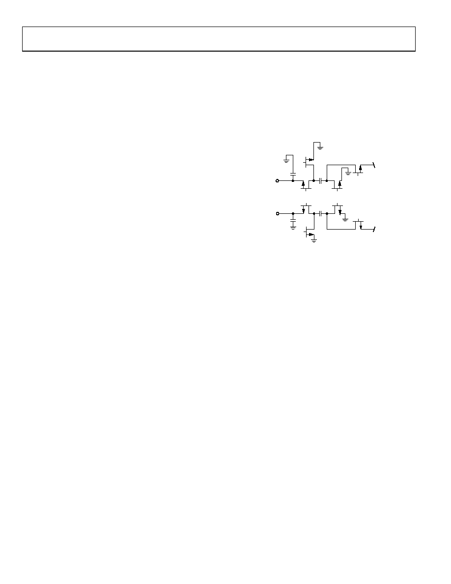
ANALOG INPUT CONSIDERATIONS
The analog input to the AD9251 is a differential switched-
capacitor circuit designed for processing differential input
signals. This circuit can support a wide common-mode range
while maintaining excellent performance. By using an input
common-mode voltage of midsupply, users can minimize
signal-dependent errors and achieve optimum performance.
SS
H
CPAR
CSAMPLE
CPAR
VIN–x
H
SS
H
VIN+x
H
07
93
8
-00
6
Figure 38. Switched-Capacitor Input Circuit
The clock signal alternately switches the input circuit between
sample-and-hold mode (see Figure 38). When the input circuit
is switched to sample mode, the signal source must be capable
of charging the sample capacitors and settling within one-half
of a clock cycle. A small resistor in series with each input can
help reduce the peak transient current injected from the output
stage of the driving source. In addition, low Q inductors or ferrite
beads can be placed on each leg of the input to reduce high
differential capacitance at the analog inputs and, therefore,
achieve the maximum bandwidth of the ADC. Such use of low
Q inductors or ferrite beads is required when driving the converter
front end at high IF frequencies. Either a shunt capacitor or two
single-ended capacitors can be placed on the inputs to provide a
matching passive network. This ultimately creates a low-pass
filter at the input to limit unwanted broadband noise. See the
Analog Dialogue article “Transformer-Coupled Front-End for
Wideband A/D Converters” (Volume 39, April 2005) for more
information. In general, the precise values depend on the
application.
相关PDF资料 |
PDF描述 |
|---|---|
| MS27656E11F13S | CONN RCPT 13POS WALL MNT W/SCKT |
| MS3106A22-9S | CONN PLUG 3POS STRAIGHT W/SCKT |
| ADM3075EWYRZ | IC TXRX RS485/422 3.3V HD 8SOIC |
| MS27467T21B41PC | CONN PLUG 41POS STRAIGHT W/PINS |
| MS3101A22-23P | CONN RCPT 8POS FREE HNG W/PINS |
相关代理商/技术参数 |
参数描述 |
|---|---|
| AD9251BCPZ-40 | 功能描述:IC ADC 14BIT 40MSPS 64LFCSP RoHS:是 类别:集成电路 (IC) >> 数据采集 - 模数转换器 系列:- 标准包装:1 系列:- 位数:14 采样率(每秒):83k 数据接口:串行,并联 转换器数目:1 功率耗散(最大):95mW 电压电源:双 ± 工作温度:0°C ~ 70°C 安装类型:通孔 封装/外壳:28-DIP(0.600",15.24mm) 供应商设备封装:28-PDIP 包装:管件 输入数目和类型:1 个单端,双极 |
| AD9251BCPZ-65 | 功能描述:IC ADC 14BIT 65MSPS 64LFCSP RoHS:是 类别:集成电路 (IC) >> 数据采集 - 模数转换器 系列:- 标准包装:1 系列:- 位数:14 采样率(每秒):83k 数据接口:串行,并联 转换器数目:1 功率耗散(最大):95mW 电压电源:双 ± 工作温度:0°C ~ 70°C 安装类型:通孔 封装/外壳:28-DIP(0.600",15.24mm) 供应商设备封装:28-PDIP 包装:管件 输入数目和类型:1 个单端,双极 |
| AD9251BCPZ-80 | 功能描述:IC ADC 14BIT 80MSPS 64LFCSP RoHS:是 类别:集成电路 (IC) >> 数据采集 - 模数转换器 系列:- 其它有关文件:TSA1204 View All Specifications 标准包装:1 系列:- 位数:12 采样率(每秒):20M 数据接口:并联 转换器数目:2 功率耗散(最大):155mW 电压电源:模拟和数字 工作温度:-40°C ~ 85°C 安装类型:表面贴装 封装/外壳:48-TQFP 供应商设备封装:48-TQFP(7x7) 包装:Digi-Reel® 输入数目和类型:4 个单端,单极;2 个差分,单极 产品目录页面:1156 (CN2011-ZH PDF) 其它名称:497-5435-6 |
| AD9251BCPZ-80 | 制造商:Analog Devices 功能描述:IC ADC 14BIT 80MSPS LFCSP-64 制造商:Analog Devices 功能描述:IC, ADC, 14BIT, 80MSPS, LFCSP-64 |
| AD9251BCPZRL7-20 | 功能描述:IC ADC 14BIT 20MSPS 64LFCSP RoHS:是 类别:集成电路 (IC) >> 数据采集 - 模数转换器 系列:- 标准包装:1 系列:- 位数:14 采样率(每秒):83k 数据接口:串行,并联 转换器数目:1 功率耗散(最大):95mW 电压电源:双 ± 工作温度:0°C ~ 70°C 安装类型:通孔 封装/外壳:28-DIP(0.600",15.24mm) 供应商设备封装:28-PDIP 包装:管件 输入数目和类型:1 个单端,双极 |
发布紧急采购,3分钟左右您将得到回复。