- 您现在的位置:买卖IC网 > PDF目录10092 > AD9251BCPZ-20 (Analog Devices Inc)IC ADC 14BIT 20MSPS 64LFCSP PDF资料下载
参数资料
| 型号: | AD9251BCPZ-20 |
| 厂商: | Analog Devices Inc |
| 文件页数: | 19/36页 |
| 文件大小: | 0K |
| 描述: | IC ADC 14BIT 20MSPS 64LFCSP |
| 标准包装: | 1 |
| 位数: | 14 |
| 采样率(每秒): | 20M |
| 数据接口: | 串行,SPI? |
| 转换器数目: | 2 |
| 功率耗散(最大): | 77mW |
| 电压电源: | 模拟和数字 |
| 工作温度: | -40°C ~ 85°C |
| 安装类型: | 表面贴装 |
| 封装/外壳: | 64-VFQFN 裸露焊盘,CSP |
| 供应商设备封装: | 64-LFCSP-VQ(9x9) |
| 包装: | 托盘 |
| 输入数目和类型: | 4 个单端,单极;2 个差分,单极 |
第1页第2页第3页第4页第5页第6页第7页第8页第9页第10页第11页第12页第13页第14页第15页第16页第17页第18页当前第19页第20页第21页第22页第23页第24页第25页第26页第27页第28页第29页第30页第31页第32页第33页第34页第35页第36页
AD9251
Rev. A | Page 26 of 36
Jitter Considerations
High speed, high resolution ADCs are sensitive to the quality
of the clock input. The degradation in SNR from the low fre-
quency SNR (SNRLF) at a given input frequency (fINPUT) due to
jitter (tJRMS) can be calculated by
SNRHF = 10 log[(2π × fINPUT × tJRMS)2 + 10
]
)
10
/
(
LF
SNR
In the previous equation, the rms aperture jitter represents the
clock input jitter specification. IF undersampling applications
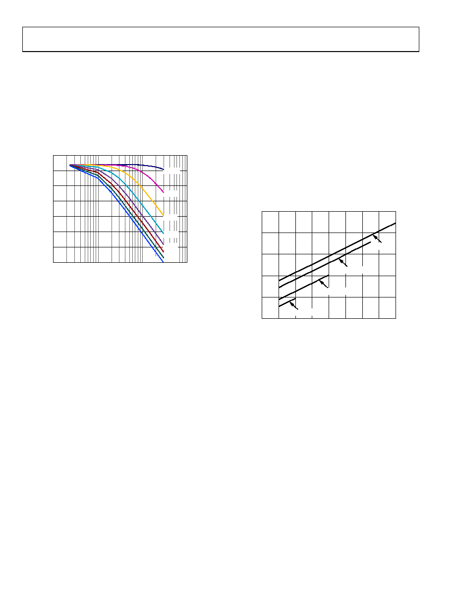
are particularly sensitive to jitter, as illustrated in Figure 56.
80
75
70
65
60
55
50
45
1
10
100
1k
FREQUENCY (MHz)
S
NR
(
d
BF
S
)
07
93
8-
0
22
0.5ps
0.2ps
0.05ps
1.0ps
1.5ps
2.0ps
2.5ps
3.0ps
Figure 56. SNR vs. Input Frequency and Jitter
The clock input should be treated as an analog signal in cases
where aperture jitter may affect the dynamic range of the AD9251.
To avoid modulating the clock signal with digital noise, keep
power supplies for clock drivers separate from the ADC output
driver supplies. Low jitter, crystal-controlled oscillators make the
best clock sources. If the clock is generated from another type of
source (by gating, dividing, or another method), it should be
retimed by the original clock at the last step.
Note available on www.analog.com for more information.
CHANNEL/CHIP SYNCHRONIZATION
The AD9251 has a SYNC input that offers the user flexible
synchronization options for synchronizing sample clocks
across multiple ADCs. The input clock divider can be enabled
to synchronize on a single occurrence of the SYNC signal or on
every occurrence. The SYNC input is internally synchronized
to the sample clock; however, to ensure there is no timing
uncertainty between multiple parts, the SYNC input signal should
be externally synchronized to the input clock signal, meeting the
setup and hold times shown in Table 5. Drive the SYNC input
using a single-ended CMOS-type signal.
POWER DISSIPATION AND STANDBY MODE
As shown in Figure 57, the analog core power dissipated by
the AD9251 is proportional to its sample rate. The digital
power dissipation of the CMOS outputs are determined
primarily by the strength of the digital drivers and the load
on each output bit.
The maximum DRVDD current (IDRVDD) can be calculated as
IDRVDD = VDRVDD × CLOAD × fCLK × N
where N is the number of output bits (30, in the case of the
AD9251).
This maximum current occurs when every output bit switches
on every clock cycle, that is, a full-scale square wave at the Nyquist
frequency of fCLK/2. In practice, the DRVDD current is estab-
lished by the average number of output bits switching, which
is determined by the sample rate and the characteristics of the
analog input signal.
Reducing the capacitive load presented to the output drivers can
minimize digital power consumption. The data in Figure 57 was
taken using the same operating conditions as those used for the
Typical Performance Characteristics, with a 5 pF load on each
output driver.
150
130
110
90
70
50
0
10
20
30
40
50
60
70
80
CLOCK RATE (MSPS)
ANAL
O
G
CO
R
E
P
O
W
E
R
(
m
W
)
07
93
8-
05
1
AD9251-80
AD9251-65
AD9251-40
AD9251-20
Figure 57. Analog Core Power vs. Clock Rate
The AD9251 is placed in power-down mode either by the SPI
port or by asserting the PDWN pin high. In this state, the ADC
typically dissipates 2.2 mW. During power-down, the output
drivers are placed in a high impedance state. Asserting the
PDWN pin low returns the AD9251 to its normal operating
mode. Note that PDWN is referenced to the digital output
driver supply (DRVDD) and should not exceed that supply
voltage.
Low power dissipation in power-down mode is achieved by
shutting down the reference, reference buffer, biasing networks,
and clock. Internal capacitors are discharged when entering power-
down mode and then must be recharged when returning to normal
operation. As a result, wake-up time is related to the time spent
in power-down mode, and shorter power-down cycles result in
proportionally shorter wake-up times.
When using the SPI port interface, the user can place the ADC
in power-down mode or standby mode. Standby mode allows
the user to keep the internal reference circuitry powered when
faster wake-up times are required. See the Memory Map section
for more details.
相关PDF资料 |
PDF描述 |
|---|---|
| MS27656E11F13S | CONN RCPT 13POS WALL MNT W/SCKT |
| MS3106A22-9S | CONN PLUG 3POS STRAIGHT W/SCKT |
| ADM3075EWYRZ | IC TXRX RS485/422 3.3V HD 8SOIC |
| MS27467T21B41PC | CONN PLUG 41POS STRAIGHT W/PINS |
| MS3101A22-23P | CONN RCPT 8POS FREE HNG W/PINS |
相关代理商/技术参数 |
参数描述 |
|---|---|
| AD9251BCPZ-40 | 功能描述:IC ADC 14BIT 40MSPS 64LFCSP RoHS:是 类别:集成电路 (IC) >> 数据采集 - 模数转换器 系列:- 标准包装:1 系列:- 位数:14 采样率(每秒):83k 数据接口:串行,并联 转换器数目:1 功率耗散(最大):95mW 电压电源:双 ± 工作温度:0°C ~ 70°C 安装类型:通孔 封装/外壳:28-DIP(0.600",15.24mm) 供应商设备封装:28-PDIP 包装:管件 输入数目和类型:1 个单端,双极 |
| AD9251BCPZ-65 | 功能描述:IC ADC 14BIT 65MSPS 64LFCSP RoHS:是 类别:集成电路 (IC) >> 数据采集 - 模数转换器 系列:- 标准包装:1 系列:- 位数:14 采样率(每秒):83k 数据接口:串行,并联 转换器数目:1 功率耗散(最大):95mW 电压电源:双 ± 工作温度:0°C ~ 70°C 安装类型:通孔 封装/外壳:28-DIP(0.600",15.24mm) 供应商设备封装:28-PDIP 包装:管件 输入数目和类型:1 个单端,双极 |
| AD9251BCPZ-80 | 功能描述:IC ADC 14BIT 80MSPS 64LFCSP RoHS:是 类别:集成电路 (IC) >> 数据采集 - 模数转换器 系列:- 其它有关文件:TSA1204 View All Specifications 标准包装:1 系列:- 位数:12 采样率(每秒):20M 数据接口:并联 转换器数目:2 功率耗散(最大):155mW 电压电源:模拟和数字 工作温度:-40°C ~ 85°C 安装类型:表面贴装 封装/外壳:48-TQFP 供应商设备封装:48-TQFP(7x7) 包装:Digi-Reel® 输入数目和类型:4 个单端,单极;2 个差分,单极 产品目录页面:1156 (CN2011-ZH PDF) 其它名称:497-5435-6 |
| AD9251BCPZ-80 | 制造商:Analog Devices 功能描述:IC ADC 14BIT 80MSPS LFCSP-64 制造商:Analog Devices 功能描述:IC, ADC, 14BIT, 80MSPS, LFCSP-64 |
| AD9251BCPZRL7-20 | 功能描述:IC ADC 14BIT 20MSPS 64LFCSP RoHS:是 类别:集成电路 (IC) >> 数据采集 - 模数转换器 系列:- 标准包装:1 系列:- 位数:14 采样率(每秒):83k 数据接口:串行,并联 转换器数目:1 功率耗散(最大):95mW 电压电源:双 ± 工作温度:0°C ~ 70°C 安装类型:通孔 封装/外壳:28-DIP(0.600",15.24mm) 供应商设备封装:28-PDIP 包装:管件 输入数目和类型:1 个单端,双极 |
发布紧急采购,3分钟左右您将得到回复。