- 您现在的位置:买卖IC网 > PDF目录10092 > AD9251BCPZ-20 (Analog Devices Inc)IC ADC 14BIT 20MSPS 64LFCSP PDF资料下载
参数资料
| 型号: | AD9251BCPZ-20 |
| 厂商: | Analog Devices Inc |
| 文件页数: | 17/36页 |
| 文件大小: | 0K |
| 描述: | IC ADC 14BIT 20MSPS 64LFCSP |
| 标准包装: | 1 |
| 位数: | 14 |
| 采样率(每秒): | 20M |
| 数据接口: | 串行,SPI? |
| 转换器数目: | 2 |
| 功率耗散(最大): | 77mW |
| 电压电源: | 模拟和数字 |
| 工作温度: | -40°C ~ 85°C |
| 安装类型: | 表面贴装 |
| 封装/外壳: | 64-VFQFN 裸露焊盘,CSP |
| 供应商设备封装: | 64-LFCSP-VQ(9x9) |
| 包装: | 托盘 |
| 输入数目和类型: | 4 个单端,单极;2 个差分,单极 |
第1页第2页第3页第4页第5页第6页第7页第8页第9页第10页第11页第12页第13页第14页第15页第16页当前第17页第18页第19页第20页第21页第22页第23页第24页第25页第26页第27页第28页第29页第30页第31页第32页第33页第34页第35页第36页
AD9251
Rev. A | Page 24 of 36
External Reference Operation
The use of an external reference may be necessary to enhance
the gain accuracy of the ADC or improve thermal drift charac-
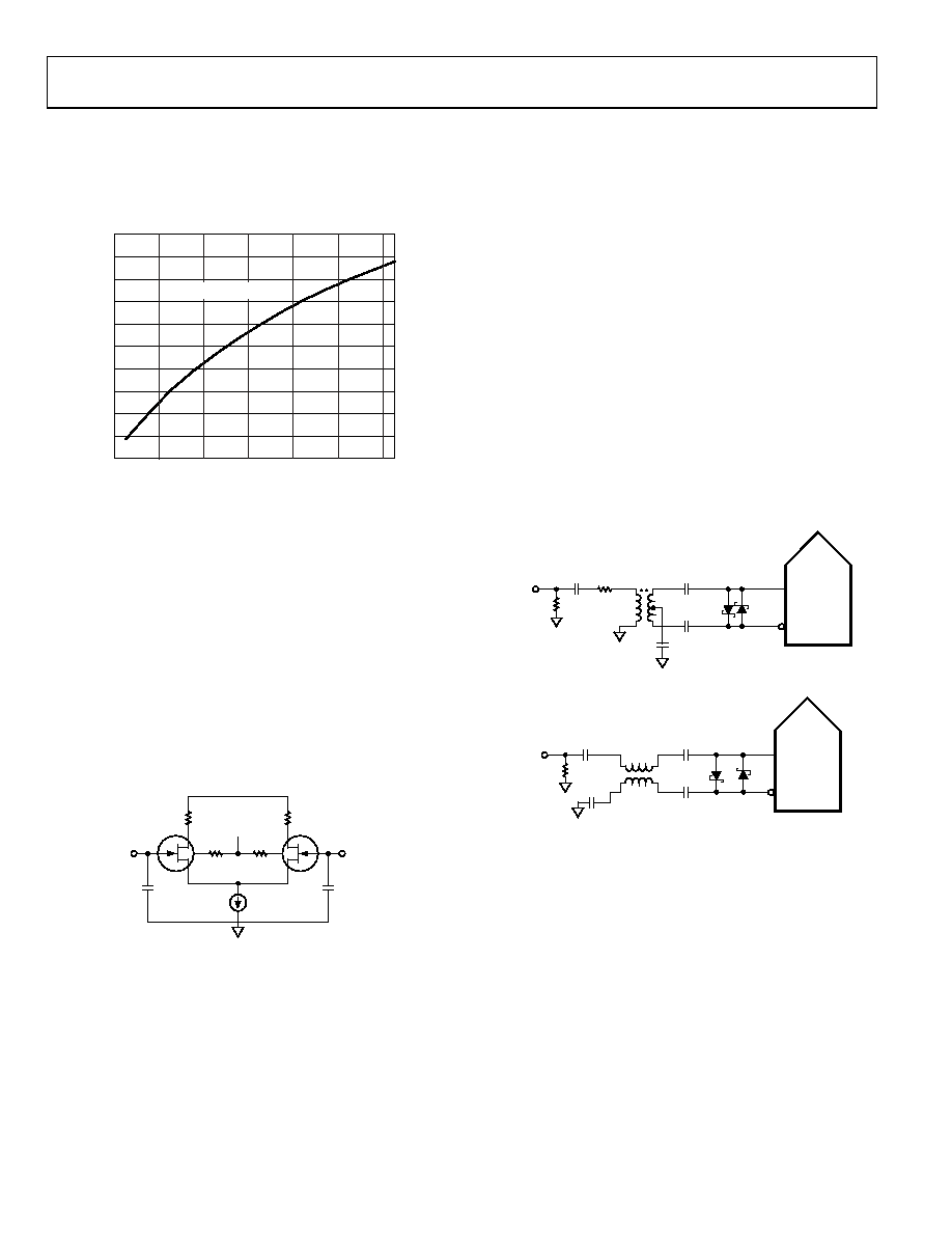
teristics. Figure 48 shows the typical drift characteristics of the
internal reference in 1.0 V mode.
4
3
2
1
0
–1
–2
–3
–4
–5
–6
–40
–20
0
20
40
60
80
TEMPERATURE (°C)
V
RE
F
E
RRO
R
(m
V
)
07
938
-05
2
VREF ERROR (mV)
Figure 48. Typical VREF Drift
When the SENSE pin is tied to AVDD, the internal reference is
disabled, allowing the use of an external reference. An internal
reference buffer loads the external reference with an equivalent
7.5 kΩ load (see Figure 37). The internal buffer generates the
positive and negative full-scale references for the ADC core.
Therefore, the external reference must be limited to a maximum
of 1.0 V.
CLOCK INPUT CONSIDERATIONS
For optimum performance, clock the AD9251 sample clock
inputs, CLK+ and CLK, with a differential signal. The signal
is typically ac-coupled into the CLK+ and CLK pins via a
transformer or capacitors. These pins are biased internally
(see Figure 49) and require no external bias.
0.9V
AVDD
2pF
CLK–
CLK+
0
79
38-
0
16
Figure 49. Equivalent Clock Input Circuit
Clock Input Options
The AD9251 has a very flexible clock input structure. The clock
input can be a CMOS, LVDS, LVPECL, or sine wave signal.
Regardless of the type of signal being used, clock source jitter is
of the most concern, as described in the Jitter Considerations
section.
ing the AD9251 (at clock rates up to 625 MHz). A low jitter clock
source is converted from a single-ended signal to a differential
signal using either an RF transformer or an RF balun.
The RF balun configuration is recommended for clock frequencies
between 125 MHz and 625 MHz, and the RF transformer is recom-
mended for clock frequencies from 10 MHz to 200 MHz. The
back-to-back Schottky diodes across the transformer/balun
secondary limit clock excursions into the AD9251 to
approximately 0.8 V p-p differential.
This limit helps prevent the large voltage swings of the clock
from feeding through to other portions of the AD9251 while
preserving the fast rise and fall times of the signal that are critical
to a low jitter performance.
0.1F
SCHOTTKY
DIODES:
HSMS2822
CLOCK
INPUT
50
100
CLK–
CLK+
ADC
Mini-Circuits
ADT1-1WT, 1:1 Z
XFMR
07
93
8-
01
7
Figure 50. Transformer-Coupled Differential Clock (Up to 200 MHz)
0.1F
1nF
CLOCK
INPUT
1nF
50
CLK–
CLK+
SCHOTTKY
DIODES:
HSMS2822
07
93
8-
01
8
ADC
Figure 51. Balun-Coupled Differential Clock (Up to 625 MHz)
相关PDF资料 |
PDF描述 |
|---|---|
| MS27656E11F13S | CONN RCPT 13POS WALL MNT W/SCKT |
| MS3106A22-9S | CONN PLUG 3POS STRAIGHT W/SCKT |
| ADM3075EWYRZ | IC TXRX RS485/422 3.3V HD 8SOIC |
| MS27467T21B41PC | CONN PLUG 41POS STRAIGHT W/PINS |
| MS3101A22-23P | CONN RCPT 8POS FREE HNG W/PINS |
相关代理商/技术参数 |
参数描述 |
|---|---|
| AD9251BCPZ-40 | 功能描述:IC ADC 14BIT 40MSPS 64LFCSP RoHS:是 类别:集成电路 (IC) >> 数据采集 - 模数转换器 系列:- 标准包装:1 系列:- 位数:14 采样率(每秒):83k 数据接口:串行,并联 转换器数目:1 功率耗散(最大):95mW 电压电源:双 ± 工作温度:0°C ~ 70°C 安装类型:通孔 封装/外壳:28-DIP(0.600",15.24mm) 供应商设备封装:28-PDIP 包装:管件 输入数目和类型:1 个单端,双极 |
| AD9251BCPZ-65 | 功能描述:IC ADC 14BIT 65MSPS 64LFCSP RoHS:是 类别:集成电路 (IC) >> 数据采集 - 模数转换器 系列:- 标准包装:1 系列:- 位数:14 采样率(每秒):83k 数据接口:串行,并联 转换器数目:1 功率耗散(最大):95mW 电压电源:双 ± 工作温度:0°C ~ 70°C 安装类型:通孔 封装/外壳:28-DIP(0.600",15.24mm) 供应商设备封装:28-PDIP 包装:管件 输入数目和类型:1 个单端,双极 |
| AD9251BCPZ-80 | 功能描述:IC ADC 14BIT 80MSPS 64LFCSP RoHS:是 类别:集成电路 (IC) >> 数据采集 - 模数转换器 系列:- 其它有关文件:TSA1204 View All Specifications 标准包装:1 系列:- 位数:12 采样率(每秒):20M 数据接口:并联 转换器数目:2 功率耗散(最大):155mW 电压电源:模拟和数字 工作温度:-40°C ~ 85°C 安装类型:表面贴装 封装/外壳:48-TQFP 供应商设备封装:48-TQFP(7x7) 包装:Digi-Reel® 输入数目和类型:4 个单端,单极;2 个差分,单极 产品目录页面:1156 (CN2011-ZH PDF) 其它名称:497-5435-6 |
| AD9251BCPZ-80 | 制造商:Analog Devices 功能描述:IC ADC 14BIT 80MSPS LFCSP-64 制造商:Analog Devices 功能描述:IC, ADC, 14BIT, 80MSPS, LFCSP-64 |
| AD9251BCPZRL7-20 | 功能描述:IC ADC 14BIT 20MSPS 64LFCSP RoHS:是 类别:集成电路 (IC) >> 数据采集 - 模数转换器 系列:- 标准包装:1 系列:- 位数:14 采样率(每秒):83k 数据接口:串行,并联 转换器数目:1 功率耗散(最大):95mW 电压电源:双 ± 工作温度:0°C ~ 70°C 安装类型:通孔 封装/外壳:28-DIP(0.600",15.24mm) 供应商设备封装:28-PDIP 包装:管件 输入数目和类型:1 个单端,双极 |
发布紧急采购,3分钟左右您将得到回复。