- 您现在的位置:买卖IC网 > PDF目录1986 > AD9271BSVZ-40 (Analog Devices Inc)IC ADC OCT 12BIT 40MSPS 100-TQFP PDF资料下载
参数资料
| 型号: | AD9271BSVZ-40 |
| 厂商: | Analog Devices Inc |
| 文件页数: | 1/60页 |
| 文件大小: | 0K |
| 描述: | IC ADC OCT 12BIT 40MSPS 100-TQFP |
| 标准包装: | 1 |
| 位数: | 12 |
| 采样率(每秒): | 40M |
| 数据接口: | 串行,SPI? |
| 转换器数目: | 8 |
| 功率耗散(最大): | 1.28W |
| 电压电源: | 单电源 |
| 工作温度: | -40°C ~ 85°C |
| 安装类型: | 表面贴装 |
| 封装/外壳: | 100-TQFP 裸露焊盘 |
| 供应商设备封装: | 100-TQFP-EP(14x14) |
| 包装: | 托盘 |
| 输入数目和类型: | 8 个单端,单极;8 个差分,单极 |
当前第1页第2页第3页第4页第5页第6页第7页第8页第9页第10页第11页第12页第13页第14页第15页第16页第17页第18页第19页第20页第21页第22页第23页第24页第25页第26页第27页第28页第29页第30页第31页第32页第33页第34页第35页第36页第37页第38页第39页第40页第41页第42页第43页第44页第45页第46页第47页第48页第49页第50页第51页第52页第53页第54页第55页第56页第57页第58页第59页第60页
Octal LNA/VGA/AAF/ADC
and Crosspoint Switch
AD9271
Rev. B
Information furnished by Analog Devices is believed to be accurate and reliable. However, no
responsibilityis assumedbyAnalogDevicesforitsuse,norforanyinfringementsof patentsorother
rightsofthirdpartiesthatmayresultfromitsuse.Specificationssubjecttochangewithoutnotice.No
license is granted by implication or otherwise under any patent or patent rights of Analog Devices.
Trademarksandregisteredtrademarksarethepropertyoftheirrespectiveowners.
One Technology Way, P.O. Box 9106, Norwood, MA 02062-9106, U.S.A.
Tel: 781.329.4700
www.analog.com
Fax: 781.461.3113
2007–2009 Analog Devices, Inc. All rights reserved.
FEATURES
8 channels of LNA, VGA, AAF, and ADC
Low noise preamplifier (LNA)
Input-referred noise = 1.1 nV/√Hz @ 5 MHz typical,
gain = 18 dB
SPI-programmable gain = 14 dB/15.6 dB/18 dB
Single-ended input; VIN maximum = 400 mV p-p/
333 mV p-p/250 mV p-p
Dual-mode active input impedance matching
Bandwidth (BW) > 70 MHz
Full-scale (FS) output = 2 V p-p differential
Variable gain amplifier (VGA)
Gain range = 6 dB to +24 dB
Linear-in-dB gain control
Antialiasing filter (AAF)
3rd-order Butterworth cutoff
Programmable from 8 MHz to 18 MHz
Analog-to-digital converter (ADC)
12 bits at 10 MSPS to 50 MSPS
SNR = 70 dB
SFDR = 80 dB
Serial LVDS (ANSI-644, IEEE 1596.3 reduced range link)
Data and frame clock outputs
Includes crosspoint switch to support
continuous wave (CW) Doppler
Low power, 150 mW per channel at 12 bits/40 MSPS (TGC)
90 mW per channel in CW Doppler
Single 1.8 V supply (3.3 V supply for CW Doppler output bias)
Flexible power-down modes
Overload recovery in <10 ns
Fast recovery from low power standby mode, <2 μs
100-lead TQFP
APPLICATIONS
Medical imaging/ultrasound
Automotive radar
GENERAL DESCRIPTION
The AD9271 is designed for low cost, low power, small size,
and ease of use. It contains eight channels of a variable gain amp-
lifier (VGA) with low noise preamplifier (LNA); an antialiasing
filter (AAF); and a 12-bit, 10 MSPS to 50 MSPS analog-to-digital
converter (ADC).
Each channel features a variable gain range of 30 dB, a fully
differential signal path, an active input preamplifier termination, a
maximum gain of up to 40 dB, and an ADC with a conversion
rate of up to 50 MSPS. The channel is optimized for dynamic
performance and low power in applications where a small
package size is critical.
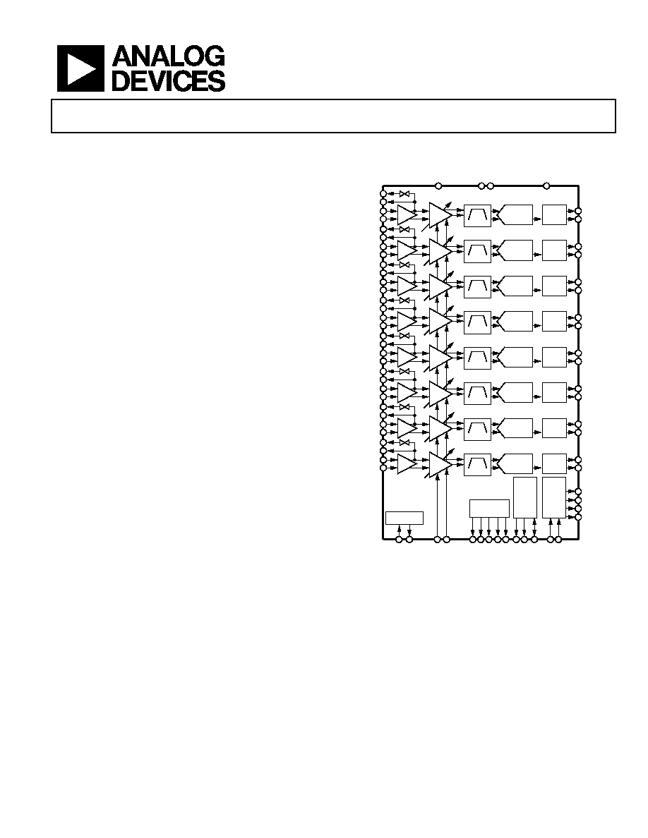
FUNCTIONAL BLOCK DIAGRAM
SER
IA
L
PO
RT
IN
TE
R
F
A
C
E
REFERENCE
FCO+
FCO–
DCO+
DCO–
LNA
LO-H
LOSW-H
LI-H
LG-H
12-BIT
ADC
SERIAL
LVDS
DOUTH+
DOUTH–
LNA
LO-G
LOSW-G
LI-G
LG-G
12-BIT
ADC
SERIAL
LVDS
DOUTG+
DOUTG–
LNA
LO-F
LOSW-F
LI-F
LG-F
12-BIT
ADC
SERIAL
LVDS
DOUTF+
DOUTF–
LNA
LO-E
LOSW-E
LI-E
LG-E
12-BIT
ADC
SERIAL
LVDS
DOUTE+
DOUTE–
LNA
LO-D
LOSW-D
LI-D
LG-D
12-BIT
ADC
SERIAL
LVDS
DOUTD+
DOUTD–
LNA
LO-C
LOSW-C
LI-C
LG-C
12-BIT
ADC
SERIAL
LVDS
DOUTC+
DOUTC–
LNA
LO-B
LOSW-B
LI-B
LG-B
LNA
LO-A
LOSW-A
LI-A
LG-A
12-BIT
ADC
SERIAL
LVDS
DOUTB+
DOUTB–
12-BIT
ADC
SERIAL
LVDS
DOUTA+
DOUTA–
AV
D
ST
BY
DR
V
DD
PDW
N
CL
K
–
CL
K
+
SD
IO
SCL
K
CSB
RB
IAS
RE
F
T
RE
F
B
VR
EF
SE
N
SE
GA
IN
+
GA
IN
–
C
W
D[5:
0]+
/–
CW
V
D
SWITCH
ARRAY
DA
T
A
RAT
E
M
U
LT
IP
LI
E
R
06
304-
0
01
AAF
AD9271
VGA
Figure 1.
The LNA has a single-ended-to-differential gain that is selectable
through the SPI. The LNA input noise is typically 1.2 nV/√Hz,
and the combined input-referred noise of the entire channel
is 1.4 nV/√Hz at maximum gain. Assuming a 15 MHz noise
bandwidth (NBW) and a 15.6 dB LNA gain, the input SNR is
roughly 86 dB. In CW Doppler mode, the LNA output drives a
transconductance amp that is switched through an 8 × 6
differential crosspoint switch. The switch is programmable
through the SPI.
相关PDF资料 |
PDF描述 |
|---|---|
| AD9280ARSRL | IC ADC 8BIT CMOS 32MSPS 28-SSOP |
| AD9281ARS | IC ADC 8BIT DUAL CMOS 28-SSOP |
| AD9283BRS-RL50 | IC ADC 8BIT 50MSPS 3V 20-SSOP |
| AD9284BCPZRL7-250 | IC ADC 8BIT 250MSPS 1.8V 48LFCSP |
| AD9286BCPZRL7-500 | IC ADC 8BIT SPI/SRL 500M 48LFCSP |
相关代理商/技术参数 |
参数描述 |
|---|---|
| AD9271BSVZ-50 | 功能描述:IC ADC 12BIT 50MSPS VGA 100-TQFP RoHS:是 类别:集成电路 (IC) >> 数据采集 - 模数转换器 系列:- 标准包装:1 系列:microPOWER™ 位数:8 采样率(每秒):1M 数据接口:串行,SPI? 转换器数目:1 功率耗散(最大):- 电压电源:模拟和数字 工作温度:-40°C ~ 125°C 安装类型:表面贴装 封装/外壳:24-VFQFN 裸露焊盘 供应商设备封装:24-VQFN 裸露焊盘(4x4) 包装:Digi-Reel® 输入数目和类型:8 个单端,单极 产品目录页面:892 (CN2011-ZH PDF) 其它名称:296-25851-6 |
| AD9271BSVZRL-25 | 功能描述:IC ADC OCT 12BIT 25MSPS 100-TQFP RoHS:是 类别:集成电路 (IC) >> 数据采集 - 模数转换器 系列:- 标准包装:1 系列:- 位数:14 采样率(每秒):83k 数据接口:串行,并联 转换器数目:1 功率耗散(最大):95mW 电压电源:双 ± 工作温度:0°C ~ 70°C 安装类型:通孔 封装/外壳:28-DIP(0.600",15.24mm) 供应商设备封装:28-PDIP 包装:管件 输入数目和类型:1 个单端,双极 |
| AD9271BSVZRL-40 | 功能描述:IC ADC OCT 12BIT 40MSPS 100-TQFP RoHS:是 类别:集成电路 (IC) >> 数据采集 - 模数转换器 系列:- 产品培训模块:Lead (SnPb) Finish for COTS Obsolescence Mitigation Program 标准包装:250 系列:- 位数:12 采样率(每秒):1.8M 数据接口:并联 转换器数目:1 功率耗散(最大):1.82W 电压电源:模拟和数字 工作温度:-40°C ~ 85°C 安装类型:表面贴装 封装/外壳:48-LQFP 供应商设备封装:48-LQFP(7x7) 包装:管件 输入数目和类型:2 个单端,单极 |
| AD9271BSVZRL-50 | 功能描述:IC ADC OCT 12BIT 50MSPS 100-TQFP RoHS:是 类别:集成电路 (IC) >> 数据采集 - 模数转换器 系列:- 产品培训模块:Lead (SnPb) Finish for COTS Obsolescence Mitigation Program 标准包装:250 系列:- 位数:12 采样率(每秒):1.8M 数据接口:并联 转换器数目:1 功率耗散(最大):1.82W 电压电源:模拟和数字 工作温度:-40°C ~ 85°C 安装类型:表面贴装 封装/外壳:48-LQFP 供应商设备封装:48-LQFP(7x7) 包装:管件 输入数目和类型:2 个单端,单极 |
| AD9271BSVZRL7-25 | 制造商:AD 制造商全称:Analog Devices 功能描述:Octal LNA/VGA/AAF/ADC and Crosspoint Switch |
发布紧急采购,3分钟左右您将得到回复。