- 您现在的位置:买卖IC网 > PDF目录1986 > AD9271BSVZ-40 (Analog Devices Inc)IC ADC OCT 12BIT 40MSPS 100-TQFP PDF资料下载
参数资料
| 型号: | AD9271BSVZ-40 |
| 厂商: | Analog Devices Inc |
| 文件页数: | 18/60页 |
| 文件大小: | 0K |
| 描述: | IC ADC OCT 12BIT 40MSPS 100-TQFP |
| 标准包装: | 1 |
| 位数: | 12 |
| 采样率(每秒): | 40M |
| 数据接口: | 串行,SPI? |
| 转换器数目: | 8 |
| 功率耗散(最大): | 1.28W |
| 电压电源: | 单电源 |
| 工作温度: | -40°C ~ 85°C |
| 安装类型: | 表面贴装 |
| 封装/外壳: | 100-TQFP 裸露焊盘 |
| 供应商设备封装: | 100-TQFP-EP(14x14) |
| 包装: | 托盘 |
| 输入数目和类型: | 8 个单端,单极;8 个差分,单极 |
第1页第2页第3页第4页第5页第6页第7页第8页第9页第10页第11页第12页第13页第14页第15页第16页第17页当前第18页第19页第20页第21页第22页第23页第24页第25页第26页第27页第28页第29页第30页第31页第32页第33页第34页第35页第36页第37页第38页第39页第40页第41页第42页第43页第44页第45页第46页第47页第48页第49页第50页第51页第52页第53页第54页第55页第56页第57页第58页第59页第60页
AD9271
Rev. B | Page 25 of
60
LNA INPUT-REFERRED
NOISE FLOOR
(5.4V rms) @ AAF BW = 15MHz
LNA + VGA NOISE = 1.4nV/ Hz
Crosspoint Switch
Each LNA is followed by a transconductance amp for V/I con-
version. Currents can be routed to one of six pairs of differential
outputs or to 12 single-ended outputs for summing. Each CWD
output pin sinks 2.4 mA dc current, and the signal has a full-scale
current of ±2 mA for each channel selected by the crosspoint
switch. For example, if four channels were to be summed on
one CWD output, the output would sink 9.6 mA dc and have a
full-scale current output of ±8 mA. The maximum number of
channels combined must be considered when setting the load
impedance for I/V conversion to ensure that the full-scale swing
and common-mode voltage are within the operating limits of
the AD9271. When interfacing to the AD8339, a common-
mode voltage of 2.5 V and a full-scale swing of 2.8 V p-p are
desired. This can be accomplished by connecting an inductor
between each CWD output and a 2.5 V supply, and then
connecting either a single-ended or differential load resistance
to the CWD± outputs. The value of resistance should be
calculated based on the maximum number of channels that can
be combined.
CWD± outputs are required under full-scale swing to be greater
than 1.5 V and less than CWVDD (3.3 V supply).
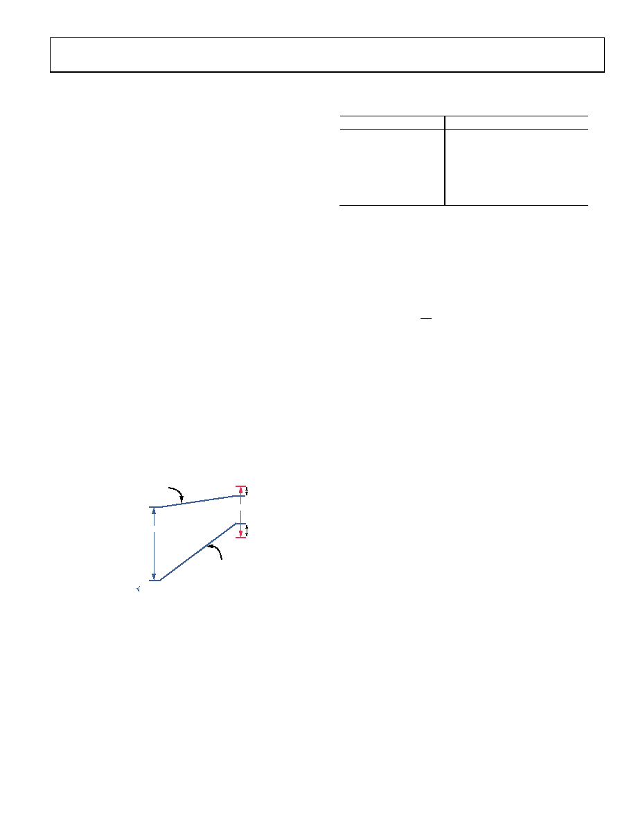
TGC OPERATION
The TGC signal path is fully differential throughout to maximize
signal swing and reduce even-order distortion; however, the LNAs
are designed to be driven from a single-ended signal source. Gain
values are referenced from the single-ended LNA input to the
differential ADC input. A simple exercise in understanding the
maximum and minimum gain requirements is shown in Figure 48.
LNA FS
(0.333V p-p SE)
ADC FS (2V p-p)
~5dB MARGIN
>8dB MARGIN
ADC NOISE FLOOR
(224V rms)
MINIMUM GAIN
MAXIMUM GAIN
063
04-
09
7
LNA
ADC
70dB
87dB
VGA GAIN RANGE > 30dB
MAX CHANNEL GAIN > 40dB
Figure 48. Gain Requirements of TGC for a 12-Bit, 40 MSPS ADC
In summary, the maximum gain required is determined by
(ADC Noise Floor/VGA Input Noise Floor) + Margin =
20 log(224/5.4) + 8 dB = 40.3 dB
The minimum gain required is determined by
(ADC Input FS/VGA Input FS) + Margin =
20 log(2/0.333) – 5 dB = 10.6 dB
Therefore, a 12-bit, 40 MSPS ADC with 15 MHz of bandwidth
should suffice in achieving the dynamic range required for most
of today’s ultrasound systems.
The system gain is distributed as listed in Table 8.
Table 8. Channel Gain Distribution
Section
Nominal Gain (dB)
LNA
14/15.6/18
Attenuator
0 to 30
VGA Amp
24
Filter
0
ADC
0
Total
8.4 to 38.4/10 to 40/12.4 to 42.4
The linear-in-dB gain (law conformance) range of the TGC path
is 30 dB, extending from 10 dB to 40 dB. The slope of the gain
control interface is 31.6 dB/V, and the gain control range is 0 V
to 1 V as specified in Equation 3. Equation 4 is the expression
for channel gain.
5
.
0
)
(
)
(
)
(
+
+
=
GAIN
V
GAIN
(3)
ICPT
V
dB
Gain
GAIN +
=
V
dB
6
.
31
)
(
(4)
where ICPT is the intercept point of the TGC gain.
In its default condition, the LNA has a gain of 15.6 dB (6×) and
the VGA gain is 6 dB if the voltage on the GAIN± pins is 0 V.
This gives rise to a total gain (or ICPT) of 10 dB through the
TGC path if the LNA input is unmatched, or of 4 dB if the LNA
is matched to 50 Ω (RFB = 200 Ω). If the voltage on the GAIN±
pins is 1 V, however, the VGA gain is 24 dB. This gives rise to a
total gain of 40 dB through the TGC path if the LNA input is
unmatched, or of 34 dB if the LNA input is matched.
Each LNA output is dc-coupled to a VGA input. The VGA consists
of an attenuator with a range of 30 dB followed by an amplifier
with 24 dB of gain for a net gain range of 6 dB to +24 dB. The
X-AMP gain-interpolation technique results in low gain error
and uniform bandwidth, and differential signal paths minimize
distortion.
At low gains, the VGA should limit the system noise perfor-
mance (SNR); at high gains, the noise is defined by the source and
LNA. The maximum voltage swing is bound by the full-scale
peak-to-peak ADC input voltage (2 V p-p).
Both the LNA and VGA have limitations within each section of
the TGC path, depending on the voltage applied to the GAIN+ and
GAIN pins. The LNA has three limitations, or full-scale settings,
depending on the gain selection applied through the SPI interface.
When a voltage of 0.2 V or less is applied to the GAIN± pins, the
LNA operates near the full-scale input range to maximize the
dynamic range of the ADC without clipping the signal. When
more than 0.2 V is applied to the GAIN± pins, the input signal to
the LNA must be lowered to keep it within the full-scale range
of the ADC (see Figure 49).
相关PDF资料 |
PDF描述 |
|---|---|
| AD9280ARSRL | IC ADC 8BIT CMOS 32MSPS 28-SSOP |
| AD9281ARS | IC ADC 8BIT DUAL CMOS 28-SSOP |
| AD9283BRS-RL50 | IC ADC 8BIT 50MSPS 3V 20-SSOP |
| AD9284BCPZRL7-250 | IC ADC 8BIT 250MSPS 1.8V 48LFCSP |
| AD9286BCPZRL7-500 | IC ADC 8BIT SPI/SRL 500M 48LFCSP |
相关代理商/技术参数 |
参数描述 |
|---|---|
| AD9271BSVZ-50 | 功能描述:IC ADC 12BIT 50MSPS VGA 100-TQFP RoHS:是 类别:集成电路 (IC) >> 数据采集 - 模数转换器 系列:- 标准包装:1 系列:microPOWER™ 位数:8 采样率(每秒):1M 数据接口:串行,SPI? 转换器数目:1 功率耗散(最大):- 电压电源:模拟和数字 工作温度:-40°C ~ 125°C 安装类型:表面贴装 封装/外壳:24-VFQFN 裸露焊盘 供应商设备封装:24-VQFN 裸露焊盘(4x4) 包装:Digi-Reel® 输入数目和类型:8 个单端,单极 产品目录页面:892 (CN2011-ZH PDF) 其它名称:296-25851-6 |
| AD9271BSVZRL-25 | 功能描述:IC ADC OCT 12BIT 25MSPS 100-TQFP RoHS:是 类别:集成电路 (IC) >> 数据采集 - 模数转换器 系列:- 标准包装:1 系列:- 位数:14 采样率(每秒):83k 数据接口:串行,并联 转换器数目:1 功率耗散(最大):95mW 电压电源:双 ± 工作温度:0°C ~ 70°C 安装类型:通孔 封装/外壳:28-DIP(0.600",15.24mm) 供应商设备封装:28-PDIP 包装:管件 输入数目和类型:1 个单端,双极 |
| AD9271BSVZRL-40 | 功能描述:IC ADC OCT 12BIT 40MSPS 100-TQFP RoHS:是 类别:集成电路 (IC) >> 数据采集 - 模数转换器 系列:- 产品培训模块:Lead (SnPb) Finish for COTS Obsolescence Mitigation Program 标准包装:250 系列:- 位数:12 采样率(每秒):1.8M 数据接口:并联 转换器数目:1 功率耗散(最大):1.82W 电压电源:模拟和数字 工作温度:-40°C ~ 85°C 安装类型:表面贴装 封装/外壳:48-LQFP 供应商设备封装:48-LQFP(7x7) 包装:管件 输入数目和类型:2 个单端,单极 |
| AD9271BSVZRL-50 | 功能描述:IC ADC OCT 12BIT 50MSPS 100-TQFP RoHS:是 类别:集成电路 (IC) >> 数据采集 - 模数转换器 系列:- 产品培训模块:Lead (SnPb) Finish for COTS Obsolescence Mitigation Program 标准包装:250 系列:- 位数:12 采样率(每秒):1.8M 数据接口:并联 转换器数目:1 功率耗散(最大):1.82W 电压电源:模拟和数字 工作温度:-40°C ~ 85°C 安装类型:表面贴装 封装/外壳:48-LQFP 供应商设备封装:48-LQFP(7x7) 包装:管件 输入数目和类型:2 个单端,单极 |
| AD9271BSVZRL7-25 | 制造商:AD 制造商全称:Analog Devices 功能描述:Octal LNA/VGA/AAF/ADC and Crosspoint Switch |
发布紧急采购,3分钟左右您将得到回复。