- 您现在的位置:买卖IC网 > PDF目录1986 > AD9271BSVZ-40 (Analog Devices Inc)IC ADC OCT 12BIT 40MSPS 100-TQFP PDF资料下载
参数资料
| 型号: | AD9271BSVZ-40 |
| 厂商: | Analog Devices Inc |
| 文件页数: | 16/60页 |
| 文件大小: | 0K |
| 描述: | IC ADC OCT 12BIT 40MSPS 100-TQFP |
| 标准包装: | 1 |
| 位数: | 12 |
| 采样率(每秒): | 40M |
| 数据接口: | 串行,SPI? |
| 转换器数目: | 8 |
| 功率耗散(最大): | 1.28W |
| 电压电源: | 单电源 |
| 工作温度: | -40°C ~ 85°C |
| 安装类型: | 表面贴装 |
| 封装/外壳: | 100-TQFP 裸露焊盘 |
| 供应商设备封装: | 100-TQFP-EP(14x14) |
| 包装: | 托盘 |
| 输入数目和类型: | 8 个单端,单极;8 个差分,单极 |
第1页第2页第3页第4页第5页第6页第7页第8页第9页第10页第11页第12页第13页第14页第15页当前第16页第17页第18页第19页第20页第21页第22页第23页第24页第25页第26页第27页第28页第29页第30页第31页第32页第33页第34页第35页第36页第37页第38页第39页第40页第41页第42页第43页第44页第45页第46页第47页第48页第49页第50页第51页第52页第53页第54页第55页第56页第57页第58页第59页第60页
AD9271
Rev. B | Page 23 of
60
0
06
30
4-
10
3
NO
IS
E
F
IG
URE
(
d
B
)
2
4
6
8
10
12
14
16
10
100
1000
RS ()
UNTERMINATED
RESISTIVE TERMINATION
ACTIVE TERMINATION
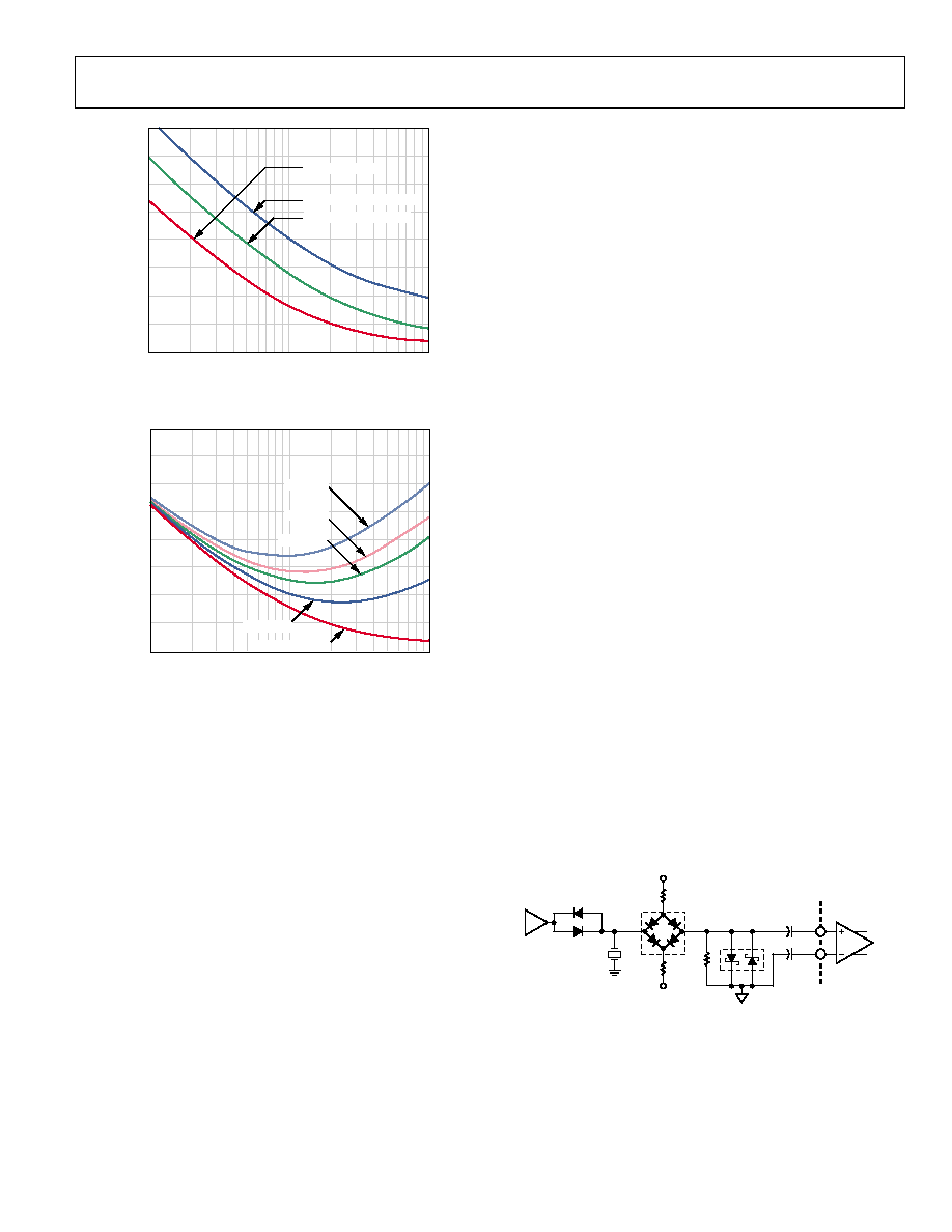
Figure 44. Noise Figure vs. RS for Resistive Termination, Active Termination
Matched, and Unterminated Inputs, VGain = 1 V, 15.6 dB LNA Gain
06
30
4-
1
0
10
100
1000
RS ()
02
2
4
6
8
10
12
14
16
NO
IS
E
F
IG
UR
E
(
d
B)
RIN = 50
RIN = 100
RIN = 75
R
= 200
IN
UNTERMINATED
Figure 45. Noise Figure vs. RS for Various Fixed Values of RIN,
Active Termination Matched Inputs, VGain = 1 V, 15.6 dB LNA Gain
The primary purpose of input impedance matching is to improve
the transient response of the system. With resistive termination, the
input noise increases due to the thermal noise of the matching
resistor and the increased contribution of the LNA’s input
voltage noise generator. With active impedance matching,
however, the contributions of both are smaller (by a factor of
1/(1 + LNA Gain)) than they would be for resistive termination.
Figure 44 shows the relative noise figure performance. In this
graph, the input impedance was swept with RS to preserve the
match at each point. The noise figures for a source impedance of
50 Ω are 7.1 dB, 4.1 dB, and 2.5 dB for the resistive termination,
active termination, and unterminated configurations, respectively.
The noise figures for 200 Ω are 4.6 dB, 2.0 dB, and 1.0 dB,
respectively.
of RIN, which is helpful for design purposes.
INPUT OVERDRIVE
Excellent overload behavior is of primary importance in ultra-
sound. Both the LNA and VGA have built-in overdrive
protection and quickly recover after an overload event.
Input Overload Protection
As with any amplifier, voltage clamping prior to the inputs is
highly recommended if the application is subject to high
transient voltages.
A block diagram of a simplified ultrasound transducer interface
is shown in Figure 46. A common transducer element serves the
dual functions of transmitting and receiving ultrasound energy.
During the transmitting phase, high voltage pulses are applied
to the ceramic elements. A typical transmit/receive (T/R) switch
can consist of four high voltage diodes in a bridge configuration.
Although the diodes ideally block transmit pulses from the
sensitive receiver input, diode characteristics are not ideal, and
resulting leakage transients imposed on the LI-x inputs can be
problematic.
Because ultrasound is a pulse system and time-of-flight is used
to determine depth, quick recovery from input overloads is
essential. Overload can occur in the preamp and the VGA.
Immediately following a transmit pulse, the typical VGA gains
are low, and the LNA is subject to overload from T/R switch
leakage. With increasing gain, the VGA can become overloaded
due to strong echoes that occur near field echoes and
acoustically dense materials, such as bone.
Figure 46 illustrates an external overload protection scheme. A
pair of back-to-back Schottky diodes is installed prior to installing
the ac-coupling capacitors. Although the BAS40 diodes are shown,
any diode is prone to exhibiting some amount of shot noise. Many
types of diodes are available for achieving the desired noise per-
formance. The configuration shown in Figure 46 tends to add
2 nV/√Hz of input-referred noise. Decreasing the 5 kΩ resistor
and increasing the 2 kΩ resistor may improve noise contribution,
depending on the application. With the diodes shown in Figure 46,
clamping levels of ±0.5 V or less significantly enhance the
overload performance of the system.
0
63
04
-10
0
TRANSDUCER
10nF
2k
5k
5k
AD9271
Tx
DRIVER
HV
BAS40-04
+5V
–5V
LNA
Figure 46. Input Overload Protection
相关PDF资料 |
PDF描述 |
|---|---|
| AD9280ARSRL | IC ADC 8BIT CMOS 32MSPS 28-SSOP |
| AD9281ARS | IC ADC 8BIT DUAL CMOS 28-SSOP |
| AD9283BRS-RL50 | IC ADC 8BIT 50MSPS 3V 20-SSOP |
| AD9284BCPZRL7-250 | IC ADC 8BIT 250MSPS 1.8V 48LFCSP |
| AD9286BCPZRL7-500 | IC ADC 8BIT SPI/SRL 500M 48LFCSP |
相关代理商/技术参数 |
参数描述 |
|---|---|
| AD9271BSVZ-50 | 功能描述:IC ADC 12BIT 50MSPS VGA 100-TQFP RoHS:是 类别:集成电路 (IC) >> 数据采集 - 模数转换器 系列:- 标准包装:1 系列:microPOWER™ 位数:8 采样率(每秒):1M 数据接口:串行,SPI? 转换器数目:1 功率耗散(最大):- 电压电源:模拟和数字 工作温度:-40°C ~ 125°C 安装类型:表面贴装 封装/外壳:24-VFQFN 裸露焊盘 供应商设备封装:24-VQFN 裸露焊盘(4x4) 包装:Digi-Reel® 输入数目和类型:8 个单端,单极 产品目录页面:892 (CN2011-ZH PDF) 其它名称:296-25851-6 |
| AD9271BSVZRL-25 | 功能描述:IC ADC OCT 12BIT 25MSPS 100-TQFP RoHS:是 类别:集成电路 (IC) >> 数据采集 - 模数转换器 系列:- 标准包装:1 系列:- 位数:14 采样率(每秒):83k 数据接口:串行,并联 转换器数目:1 功率耗散(最大):95mW 电压电源:双 ± 工作温度:0°C ~ 70°C 安装类型:通孔 封装/外壳:28-DIP(0.600",15.24mm) 供应商设备封装:28-PDIP 包装:管件 输入数目和类型:1 个单端,双极 |
| AD9271BSVZRL-40 | 功能描述:IC ADC OCT 12BIT 40MSPS 100-TQFP RoHS:是 类别:集成电路 (IC) >> 数据采集 - 模数转换器 系列:- 产品培训模块:Lead (SnPb) Finish for COTS Obsolescence Mitigation Program 标准包装:250 系列:- 位数:12 采样率(每秒):1.8M 数据接口:并联 转换器数目:1 功率耗散(最大):1.82W 电压电源:模拟和数字 工作温度:-40°C ~ 85°C 安装类型:表面贴装 封装/外壳:48-LQFP 供应商设备封装:48-LQFP(7x7) 包装:管件 输入数目和类型:2 个单端,单极 |
| AD9271BSVZRL-50 | 功能描述:IC ADC OCT 12BIT 50MSPS 100-TQFP RoHS:是 类别:集成电路 (IC) >> 数据采集 - 模数转换器 系列:- 产品培训模块:Lead (SnPb) Finish for COTS Obsolescence Mitigation Program 标准包装:250 系列:- 位数:12 采样率(每秒):1.8M 数据接口:并联 转换器数目:1 功率耗散(最大):1.82W 电压电源:模拟和数字 工作温度:-40°C ~ 85°C 安装类型:表面贴装 封装/外壳:48-LQFP 供应商设备封装:48-LQFP(7x7) 包装:管件 输入数目和类型:2 个单端,单极 |
| AD9271BSVZRL7-25 | 制造商:AD 制造商全称:Analog Devices 功能描述:Octal LNA/VGA/AAF/ADC and Crosspoint Switch |
发布紧急采购,3分钟左右您将得到回复。