- 您现在的位置:买卖IC网 > PDF目录1986 > AD9271BSVZ-40 (Analog Devices Inc)IC ADC OCT 12BIT 40MSPS 100-TQFP PDF资料下载
参数资料
| 型号: | AD9271BSVZ-40 |
| 厂商: | Analog Devices Inc |
| 文件页数: | 19/60页 |
| 文件大小: | 0K |
| 描述: | IC ADC OCT 12BIT 40MSPS 100-TQFP |
| 标准包装: | 1 |
| 位数: | 12 |
| 采样率(每秒): | 40M |
| 数据接口: | 串行,SPI? |
| 转换器数目: | 8 |
| 功率耗散(最大): | 1.28W |
| 电压电源: | 单电源 |
| 工作温度: | -40°C ~ 85°C |
| 安装类型: | 表面贴装 |
| 封装/外壳: | 100-TQFP 裸露焊盘 |
| 供应商设备封装: | 100-TQFP-EP(14x14) |
| 包装: | 托盘 |
| 输入数目和类型: | 8 个单端,单极;8 个差分,单极 |
第1页第2页第3页第4页第5页第6页第7页第8页第9页第10页第11页第12页第13页第14页第15页第16页第17页第18页当前第19页第20页第21页第22页第23页第24页第25页第26页第27页第28页第29页第30页第31页第32页第33页第34页第35页第36页第37页第38页第39页第40页第41页第42页第43页第44页第45页第46页第47页第48页第49页第50页第51页第52页第53页第54页第55页第56页第57页第58页第59页第60页
AD9271
Rev. B | Page 26 of
60
0
0.1
0.2
0.3
0.4
0.5
0.6
0.7
0.8
0.9
1.0
06
30
4-
1
VGAIN (V)
10
IN
P
U
T
FU
L
-S
C
A
L
E
(
V
p-p)
0
0.050
0.100
0.150
0.200
0.250
0.300
0.350
0.400
0.450
LNA
GAIN = 6x
LNA GAIN = 8x
LNA GAIN = 5x
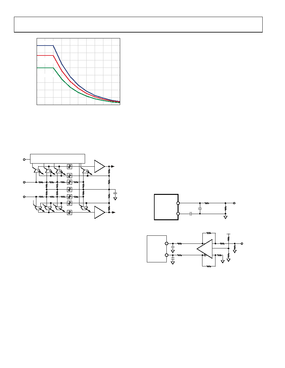
Figure 49. LNA/VGA Full-Scale Limitations
Variable Gain Amplifier
The differential X-AMP VGA provides precise input attenuation
and interpolation. It has a low input-referred noise of 4 nV/√Hz
and excellent gain linearity. A simplified block diagram is shown
in Figure 50.
VIP
GAIN
3dB
VIN
gm
06
30
4-
0
78
POSTAMP
–
POSTAMP
+
GAIN INTERPOLATOR
Figure 50. Simplified VGA Schematic
The input of the VGA is a 12-stage differential resistor ladder with
3.01 dB per tap. The resulting total gain range is 30 dB, which
allows for range loss at the endpoints. The effective input resistance
per side is 180 Ω nominally for a total differential resistance of
360 Ω. The ladder is driven by a fully differential input signal from
the LNA. LNA outputs are dc-coupled to avoid external decoupling
capacitors. The common-mode voltage of the attenuator and the
VGA is controlled by an amplifier that uses the same midsupply
voltage derived in the LNA, permitting dc coupling of the LNA
to the VGA without introducing large offsets due to common-
mode differences. However, any offset from the LNA will be
amplified as the gain is increased, producing an exponentially
increasing VGA output offset.
The input stages of the X-AMP are distributed along the ladder,
and a biasing interpolator, controlled by the gain interface,
determines the input tap point. With overlapping bias currents,
signals from successive taps merge to provide a smooth
attenuation range from 0 dB to 30 dB. This circuit technique
results in linear-in-dB gain law conformance and low distortion
levels—only deviating ±0.5 dB or less from the ideal. The gain
slope is monotonic with respect to the control voltage and is
stable with variations in process, temperature, and supply.
The X-AMP inputs are part of a 24 dB gain feedback amplifier
that completes the VGA. Its bandwidth is about 70 MHz. The
input stage is designed to reduce feedthrough to the output and
to ensure excellent frequency response uniformity across the
gain setting.
Gain Control
The gain control interface, GAIN±, is a differential input. The
VGA gain, VGAIN, is shown in Equation 3. VGAIN varies the gain
of all VGAs through the interpolator by selecting the appropriate
input stages connected to the input attenuator. The nominal
VGAIN range for 30 dB/V is 0 V to 1 V, with the best gain linearity
from about 0.1 V to 0.9 V, where the error is typically less than
±0.5 dB. For VGAIN voltages greater than 0.9 V and less than 0.1 V,
the error increases. The value of VGAIN can exceed the supply
voltage by 1 V without gain foldover.
Gain control response time is less than 750 ns to settle within 10%
of the final value for a change from minimum to maximum gain.
There are two ways in which the GAIN+ and GAIN pins can
be interfaced. Using a single-ended method, a Kelvin type of
connection to ground can be used as shown in Figure 51. For
driving multiple devices, it is preferable to use a differential
method, as shown in Figure 52. In either method, the GAIN+
and GAIN pins should be dc-coupled and driven to accom-
modate a 1 V full-scale input.
AD9271
GAIN+
GAIN–
100
0 TO 1V DC
50
0.01F
06
304
-10
9
KELVIN
CONNECTION
Figure 51. Single-Ended GAIN± Pins Configuration
GAIN–
50
GAIN+
AD9271
AVDD
26k
10k
0.01F
±0.25DC AT
0.5V CM
±0.25DC AT
0.5V CM
100
499
±0.5V DC
0.01F
100
499
523
499
0.5V CM
AD8138
0
63
04
-09
8
Figure 52. Differential GAIN± Pins Configuration
VGA Noise
In a typical application, a VGA compresses a wide dynamic
range input signal to within the input span of an ADC. The
input-referred noise of the LNA limits the minimum resolvable
input signal, whereas the output-referred noise, which depends
primarily on the VGA, limits the maximum instantaneous
dynamic range that can be processed at any one particular gain
control voltage. This latter limit is set in accordance with the
total noise floor of the ADC.
and Figure 25 for the short-circuit input conditions. The input
相关PDF资料 |
PDF描述 |
|---|---|
| AD9280ARSRL | IC ADC 8BIT CMOS 32MSPS 28-SSOP |
| AD9281ARS | IC ADC 8BIT DUAL CMOS 28-SSOP |
| AD9283BRS-RL50 | IC ADC 8BIT 50MSPS 3V 20-SSOP |
| AD9284BCPZRL7-250 | IC ADC 8BIT 250MSPS 1.8V 48LFCSP |
| AD9286BCPZRL7-500 | IC ADC 8BIT SPI/SRL 500M 48LFCSP |
相关代理商/技术参数 |
参数描述 |
|---|---|
| AD9271BSVZ-50 | 功能描述:IC ADC 12BIT 50MSPS VGA 100-TQFP RoHS:是 类别:集成电路 (IC) >> 数据采集 - 模数转换器 系列:- 标准包装:1 系列:microPOWER™ 位数:8 采样率(每秒):1M 数据接口:串行,SPI? 转换器数目:1 功率耗散(最大):- 电压电源:模拟和数字 工作温度:-40°C ~ 125°C 安装类型:表面贴装 封装/外壳:24-VFQFN 裸露焊盘 供应商设备封装:24-VQFN 裸露焊盘(4x4) 包装:Digi-Reel® 输入数目和类型:8 个单端,单极 产品目录页面:892 (CN2011-ZH PDF) 其它名称:296-25851-6 |
| AD9271BSVZRL-25 | 功能描述:IC ADC OCT 12BIT 25MSPS 100-TQFP RoHS:是 类别:集成电路 (IC) >> 数据采集 - 模数转换器 系列:- 标准包装:1 系列:- 位数:14 采样率(每秒):83k 数据接口:串行,并联 转换器数目:1 功率耗散(最大):95mW 电压电源:双 ± 工作温度:0°C ~ 70°C 安装类型:通孔 封装/外壳:28-DIP(0.600",15.24mm) 供应商设备封装:28-PDIP 包装:管件 输入数目和类型:1 个单端,双极 |
| AD9271BSVZRL-40 | 功能描述:IC ADC OCT 12BIT 40MSPS 100-TQFP RoHS:是 类别:集成电路 (IC) >> 数据采集 - 模数转换器 系列:- 产品培训模块:Lead (SnPb) Finish for COTS Obsolescence Mitigation Program 标准包装:250 系列:- 位数:12 采样率(每秒):1.8M 数据接口:并联 转换器数目:1 功率耗散(最大):1.82W 电压电源:模拟和数字 工作温度:-40°C ~ 85°C 安装类型:表面贴装 封装/外壳:48-LQFP 供应商设备封装:48-LQFP(7x7) 包装:管件 输入数目和类型:2 个单端,单极 |
| AD9271BSVZRL-50 | 功能描述:IC ADC OCT 12BIT 50MSPS 100-TQFP RoHS:是 类别:集成电路 (IC) >> 数据采集 - 模数转换器 系列:- 产品培训模块:Lead (SnPb) Finish for COTS Obsolescence Mitigation Program 标准包装:250 系列:- 位数:12 采样率(每秒):1.8M 数据接口:并联 转换器数目:1 功率耗散(最大):1.82W 电压电源:模拟和数字 工作温度:-40°C ~ 85°C 安装类型:表面贴装 封装/外壳:48-LQFP 供应商设备封装:48-LQFP(7x7) 包装:管件 输入数目和类型:2 个单端,单极 |
| AD9271BSVZRL7-25 | 制造商:AD 制造商全称:Analog Devices 功能描述:Octal LNA/VGA/AAF/ADC and Crosspoint Switch |
发布紧急采购,3分钟左右您将得到回复。