参数资料
| 型号: | AD9276BSVZ |
| 厂商: | Analog Devices Inc |
| 文件页数: | 18/48页 |
| 文件大小: | 0K |
| 描述: | IC ADC 12BIT LNA/VGA/AAF 100TQFP |
| 标准包装: | 1 |
| 类型: | AAF,ADC,解调器,LNA,VGA |
| 分辨率(位): | 12 b |
| 采样率(每秒): | 10M ~ 80M |
| 数据接口: | 串行,SPI? |
| 电压电源: | 模拟和数字 |
| 电源电压: | 1.8V,3V |
| 工作温度: | -40°C ~ 85°C |
| 安装类型: | 表面贴装 |
| 封装/外壳: | 100-TQFP 裸露焊盘 |
| 供应商设备封装: | 100-TQFP-EP(14x14) |
| 包装: | 托盘 |
第1页第2页第3页第4页第5页第6页第7页第8页第9页第10页第11页第12页第13页第14页第15页第16页第17页当前第18页第19页第20页第21页第22页第23页第24页第25页第26页第27页第28页第29页第30页第31页第32页第33页第34页第35页第36页第37页第38页第39页第40页第41页第42页第43页第44页第45页第46页第47页第48页
AD9276
Rev. 0 | Page 25 of 48
INPUT OVERDRIVE
Excellent overload behavior is of primary importance in
ultrasound. Both the LNA and VGA have built-in overdrive
protection and quickly recover after an overload event.
Input Overload Protection
As with any amplifier, voltage clamping prior to the inputs
is highly recommended if the application is subject to high
transient voltages.
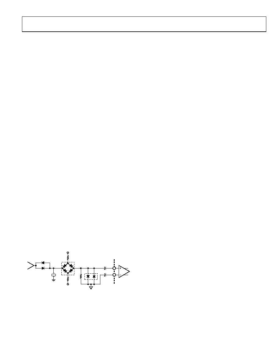
Figure 52 shows a simplified ultrasound transducer interface.
A common transducer element serves the dual functions of
transmitting and receiving ultrasound energy. During the
transmitting phase, high voltage pulses are applied to the ceramic
elements. A typical transmit/receive (T/R) switch can consist of
four high voltage diodes in a bridge configuration. Although the
diodes ideally block transmit pulses from the sensitive receiver
input, diode characteristics are not ideal, and the resulting leakage
transients imposed on the LI-x inputs can be problematic.
Because ultrasound is a pulse system and time-of-flight is used
to determine depth, quick recovery from input overloads is
essential. Overload can occur in the preamplifier and in the
VGA. Immediately following a transmit pulse, the typical VGA
gains are low, and the LNA is subject to overload from T/R
switch leakage. With increasing gain, the VGA can become
overloaded due to strong echoes that occur near field echoes
and acoustically dense materials, such as bone.
Figure 52 illustrates an external overload protection scheme. A
pair of back-to-back signal diodes should be in place prior to
the ac coupling capacitors. Keep in mind that all diodes are
prone to exhibiting some amount of shot noise. Many types of
diodes are available for achieving the desired noise performance.
The configuration shown in Figure 52 tends to add 2 nV/√Hz of
input-referred noise. Decreasing the 5 kΩ resistor and increasing
the 2 kΩ resistor may improve noise contribution, depending
on the application. With the diodes shown in Figure 52, clamp-
ing levels of ±0.5 V or less significantly enhance the overload
performance of the system.
TRANSDUCER
10nF
2k
5k
AD9276
Tx
DRIVER
HV
+5V
–5V
LNA
08
18
0-
04
6
Figure 52. Input Overload Protection
CW DOPPLER OPERATION
Each channel of the AD9276 includes an I/Q demodulator. Each
demodulator has an individual programmable phase shifter.
The I/Q demodulator is ideal for phased array beamforming
applications in medical ultrasound. Each channel can be pro-
grammed for 16 delay states (360°/16 or 22.5°/step), selectable
via the SPI port. The part has a RESET input used to synchronize
the LO dividers of each channel. If multiple AD9276s are used,
a common RESET across the array ensures synchronized phase
for all channels. Internal to the AD9276, the individual channel I
and Q outputs are current summed. If multiple AD9276s are used,
the I and Q outputs from each AD9276 can be current summed
and converted to a voltage using an external transimpedance
amplifier.
Quadrature Generation
The internal 0° and 90° LO phases are digitally generated by
a divide-by-4 logic circuit. The divider is dc-coupled and
inherently broadband; the maximum LO frequency is limited
only by its switching speed. The duty cycle of the quadrature LO
signals is intrinsically 50% and is unaffected by the asymmetry
of the externally connected 4LO input. Furthermore, the divider
is implemented such that the 4LO signal reclocks the final flip-
flops that generate the internal LO signals and thereby minimizes
noise introduced by the divide circuitry.
For optimum performance, the 4LO input is driven differentially,
as done on the AD9276 evaluation board. The common-mode
voltage on each pin is approximately 1.2 V with the nominal 3 V
supply. It is important to ensure that the LO source has very low
phase noise (jitter), fast slew rate, and adequate input level to
obtain optimum performance of the CW signal chain.
Beamforming applications require a precise channel-to-channel
phase relationship for coherence among multiple channels. A
RESET pin is provided to synchronize the LO divider circuits
in different AD9276s when they are used in arrays. The RESET
pin resets the dividers to a known state after power is applied to
multiple AD9276s. Accurate channel-to-channel phase matching
can only be achieved via a common pulse on the RESET pin when
using more than one AD9276.
相关PDF资料 |
PDF描述 |
|---|---|
| AD9277BSVZ | IC ADC 14BIT LNA/VGA/AAF 100TQFP |
| AD9278BBCZ | IC ADC 12BIT 50MSPS 144CSPBGA |
| AD9279BBCZ | IC ADC 12BIT 80MSPS 144CSPBGA |
| AD9393BBCZRL-80 | IC INTERFACE 80MHZ HDMI 76CSPBGA |
| AD9398KSTZ-150 | IC INTERFACE 150MHZ HDMI 100LQFP |
相关代理商/技术参数 |
参数描述 |
|---|---|
| AD9276XBCZ | 功能描述:IC ADC 12BIT LNA/VGA/AAF 制造商:analog devices inc. 系列:* 零件状态:上次购买时间 标准包装:1 |
| AD9276XSVZ | 功能描述:IC ADC 12BIT LNA/VGA/AAF 制造商:analog devices inc. 系列:* 零件状态:上次购买时间 标准包装:1 |
| AD9277 | 制造商:AD 制造商全称:Analog Devices 功能描述:Octal LNA/VGA/AAF/14-Bit ADC and CW I/Q Demodulator |
| AD9277-50EBZ | 功能描述:BOARD EVAL FOR AD9277 RoHS:是 类别:编程器,开发系统 >> 评估板 - 模数转换器 (ADC) 系列:- 产品培训模块:Obsolescence Mitigation Program 标准包装:1 系列:- ADC 的数量:1 位数:12 采样率(每秒):94.4k 数据接口:USB 输入范围:±VREF/2 在以下条件下的电源(标准):- 工作温度:-40°C ~ 85°C 已用 IC / 零件:MAX11645 已供物品:板,软件 |
| AD9277BSVZ | 功能描述:IC ADC 14BIT LNA/VGA/AAF 100TQFP RoHS:是 类别:集成电路 (IC) >> 数据采集 - ADCs/DAC - 专用型 系列:- 产品培训模块:Lead (SnPb) Finish for COTS Obsolescence Mitigation Program 标准包装:50 系列:- 类型:数据采集系统(DAS) 分辨率(位):16 b 采样率(每秒):21.94k 数据接口:MICROWIRE?,QSPI?,串行,SPI? 电压电源:模拟和数字 电源电压:1.8 V ~ 3.6 V 工作温度:-40°C ~ 85°C 安装类型:表面贴装 封装/外壳:40-WFQFN 裸露焊盘 供应商设备封装:40-TQFN-EP(6x6) 包装:托盘 |
发布紧急采购,3分钟左右您将得到回复。