参数资料
| 型号: | AD9276BSVZ |
| 厂商: | Analog Devices Inc |
| 文件页数: | 21/48页 |
| 文件大小: | 0K |
| 描述: | IC ADC 12BIT LNA/VGA/AAF 100TQFP |
| 标准包装: | 1 |
| 类型: | AAF,ADC,解调器,LNA,VGA |
| 分辨率(位): | 12 b |
| 采样率(每秒): | 10M ~ 80M |
| 数据接口: | 串行,SPI? |
| 电压电源: | 模拟和数字 |
| 电源电压: | 1.8V,3V |
| 工作温度: | -40°C ~ 85°C |
| 安装类型: | 表面贴装 |
| 封装/外壳: | 100-TQFP 裸露焊盘 |
| 供应商设备封装: | 100-TQFP-EP(14x14) |
| 包装: | 托盘 |
第1页第2页第3页第4页第5页第6页第7页第8页第9页第10页第11页第12页第13页第14页第15页第16页第17页第18页第19页第20页当前第21页第22页第23页第24页第25页第26页第27页第28页第29页第30页第31页第32页第33页第34页第35页第36页第37页第38页第39页第40页第41页第42页第43页第44页第45页第46页第47页第48页
AD9276
Rev. 0 | Page 28 of 48
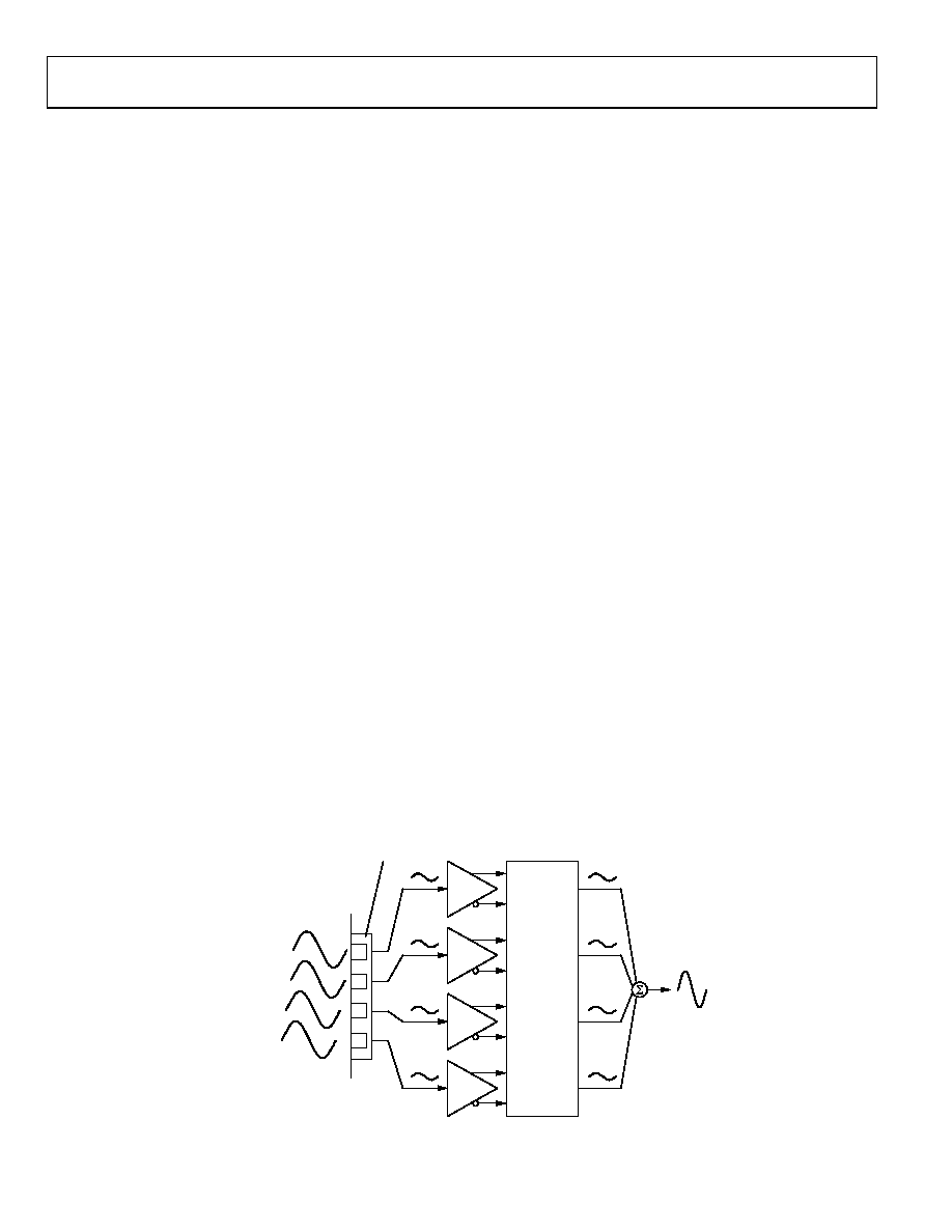
For CW Doppler operation, the AD9276 integrates the LNA,
phase shifter, frequency conversion, and I/Q demodulation
into a single package and directly yields the baseband signal.
Figure 54 is a simplified diagram showing the concept for four
channels. The ultrasound wave (US wave) is received by four
transducer elements, TE1 through TE4, in an ultrasound probe
and generates signals E1 through E4. In this example, the phase
at TE1 leads the phase at TE2 by 45°.
In a real application, the phase difference depends on the
element spacing, wavelength (λ), speed of sound, angle of
incidence, and other factors. In Figure 54, the signals E1
through E4 are amplified by the low noise amplifiers. For
optimum signal-to-noise performance, the output of the LNA
is applied directly to the input of the demodulators. To sum the
signals E1 through E4, E2 is shifted 45° relative to E1 by setting
the phase code in Channel 2 to 0010, E3 is shifted 90° (0100), and
E4 is shifted 135° (0110). The phase-aligned current signals at
the output of the AD9276 are summed in an I-to-V converter to
provide the combined output signal with a theoretical improve-
ment in dynamic range of 6 dB for the four channels.
CW Application Information
The RESET pin is used to synchronize the LO dividers when
using multiple AD9276s. Because they are driven by the same
internal LO, the channels in any AD9276 are inherently syn-
chronous. However, when multiple AD9276s are used, it is
possible for their dividers to wake up in different phase states.
The function of the RESET pin is to phase align all the LO
signals in multiple AD9276s.
The 4LO divider of each AD9276 can be initiated in one of four
possible states: 0°, 90°, 180°, and 270° relative to other AD9276s.
The internally generated I/Q signals of each AD9276 LO are always
at a 90° angle relative to each other, but a phase shift can occur
during power-up between the dividers of multiple AD9276s
used in a common array.
The RESET mechanism also allows the measurement of non-
mixing gain from the RF input to the output. The rising edge of
the active high RESET pulse can occur at any time; however, the
duration should be ≥ 20 ns minimum. When the RESET pulse
transitions from high to low, the LO dividers are reactivated on
the next rising edge of the 4LO clock. To guarantee synchronous
operation of multiple AD9276s, the RESET pulse must go low
on all devices before the next rising edge of the 4LO clock.
Therefore, it is best to have the RESET pulse go low on the falling
edge of the 4LO clock; at the very least, the tSETUP should be ≥ 5 ns.
An optimal timing setup is for the RESET pulse to go high on a
4LO falling edge and to go low on a 4LO falling edge; this gives
15 ns of setup time even at a 4LO frequency of 32 MHz (8 MHz
internal LO).
Check the synchronization of multiple AD9276s using the
following procedure:
1.
Activate at least one channel per AD9276 by setting the
appropriate channel enable bit in the serial interface (see
Table 18, Register 0x2D, Bit 4).
2.
Set the phase code of all AD9276 channels to the same
logic state, for example, 0000.
3.
Apply the same test signal to all devices to generate a sine
wave in the baseband output and measure the output of
one channel per device.
4.
Apply a RESET pulse to all AD9276s.
5.
Because all the phase codes of the AD9276s should be the
same, the combined signal of multiple devices should be N
times greater than a single channel. If the combined signal
is less than N times one channel, one or more of the LO
phases of the individual AD9276s is in error.
S1
S2
S3
S4
E1
E2
E3
E4
90°
45°
135°
0°
SUMMED
OUTPUT
S1 + S2 + S3 + S4
S1 THROUGH S4
ARE NOW
IN PHASE
PHASE BIT
SETTINGS
CH 1
PHASE SET
FOR 135°
LAG
CH 2
PHASE SET
FOR 90°
LAG
CH 3
PHASE SET
FOR 45°
LAG
CH 4
PHASE SET
FOR 0°
LAG
TRANSDUCER
ELEMENTS TE1
THROUGH TE4
CONVERT US TO
ELECTRICAL
SIGNALS
LNA
4 US WAVES
ARE DELAYED
45° EACH WITH
RESPECT TO
EACH OTHER
08
18
0-
0
48
Figure 54. Simplified Example of the AD9276 Phase Shifter
相关PDF资料 |
PDF描述 |
|---|---|
| AD9277BSVZ | IC ADC 14BIT LNA/VGA/AAF 100TQFP |
| AD9278BBCZ | IC ADC 12BIT 50MSPS 144CSPBGA |
| AD9279BBCZ | IC ADC 12BIT 80MSPS 144CSPBGA |
| AD9393BBCZRL-80 | IC INTERFACE 80MHZ HDMI 76CSPBGA |
| AD9398KSTZ-150 | IC INTERFACE 150MHZ HDMI 100LQFP |
相关代理商/技术参数 |
参数描述 |
|---|---|
| AD9276XBCZ | 功能描述:IC ADC 12BIT LNA/VGA/AAF 制造商:analog devices inc. 系列:* 零件状态:上次购买时间 标准包装:1 |
| AD9276XSVZ | 功能描述:IC ADC 12BIT LNA/VGA/AAF 制造商:analog devices inc. 系列:* 零件状态:上次购买时间 标准包装:1 |
| AD9277 | 制造商:AD 制造商全称:Analog Devices 功能描述:Octal LNA/VGA/AAF/14-Bit ADC and CW I/Q Demodulator |
| AD9277-50EBZ | 功能描述:BOARD EVAL FOR AD9277 RoHS:是 类别:编程器,开发系统 >> 评估板 - 模数转换器 (ADC) 系列:- 产品培训模块:Obsolescence Mitigation Program 标准包装:1 系列:- ADC 的数量:1 位数:12 采样率(每秒):94.4k 数据接口:USB 输入范围:±VREF/2 在以下条件下的电源(标准):- 工作温度:-40°C ~ 85°C 已用 IC / 零件:MAX11645 已供物品:板,软件 |
| AD9277BSVZ | 功能描述:IC ADC 14BIT LNA/VGA/AAF 100TQFP RoHS:是 类别:集成电路 (IC) >> 数据采集 - ADCs/DAC - 专用型 系列:- 产品培训模块:Lead (SnPb) Finish for COTS Obsolescence Mitigation Program 标准包装:50 系列:- 类型:数据采集系统(DAS) 分辨率(位):16 b 采样率(每秒):21.94k 数据接口:MICROWIRE?,QSPI?,串行,SPI? 电压电源:模拟和数字 电源电压:1.8 V ~ 3.6 V 工作温度:-40°C ~ 85°C 安装类型:表面贴装 封装/外壳:40-WFQFN 裸露焊盘 供应商设备封装:40-TQFN-EP(6x6) 包装:托盘 |
发布紧急采购,3分钟左右您将得到回复。