参数资料
| 型号: | AD9279BBCZ |
| 厂商: | Analog Devices Inc |
| 文件页数: | 17/44页 |
| 文件大小: | 0K |
| 描述: | IC ADC 12BIT 80MSPS 144CSPBGA |
| 标准包装: | 1 |
| 类型: | AAF,ADC,解调器,LNA,VGA |
| 分辨率(位): | 12 b |
| 采样率(每秒): | 80M |
| 数据接口: | 串行,SPI? |
| 电压电源: | 模拟和数字 |
| 电源电压: | 1.7 V ~ 1.9 V,2.7 V ~ 3.6 V |
| 工作温度: | -40°C ~ 85°C |
| 安装类型: | 表面贴装 |
| 封装/外壳: | 144-LFBGA,CSPBGA |
| 供应商设备封装: | 144-CSPBGA(10x10) |
| 包装: | 托盘 |
第1页第2页第3页第4页第5页第6页第7页第8页第9页第10页第11页第12页第13页第14页第15页第16页当前第17页第18页第19页第20页第21页第22页第23页第24页第25页第26页第27页第28页第29页第30页第31页第32页第33页第34页第35页第36页第37页第38页第39页第40页第41页第42页第43页第44页
AD9279
Rev. 0 | Page 24 of 44
shows an example of how to select RFB1 and RFB2 for 66 Ω, 100 Ω,
and 200 Ω input impedance for LNA gain = 21.3 dB (12×).
Table 9. Active Termination Example for LNA Gain = 21.3 dB,
RFB1 = 700 Ω, RFB2 = 1400 Ω
Register
0x2C
Value
Rs (Ω)
LO-x
Switch
LOSW-x
Switch
RFB (Ω)
RIN (Ω)
(Eq. 1)
00
(default)
100
On
Off
RFB1
100
01
50
On
RFB1||RFB2
66
10
200
Off
On
RFB2
200
11
N/A
Off
∞
The bandwidth (BW) of the LNA is greater than 100 MHz.
Ultimately, the BW of the LNA limits the accuracy of the
synthesized RIN. For RIN = RS up to about 200 Ω, the best match
is between 100 kHz and 10 MHz, where the lower frequency
limit is determined by the size of the ac coupling capacitors, and
the upper limit is determined by the LNA BW. Furthermore, the
input capacitance and RS limit the BW at higher frequencies.
09
42
3-
0
40
10
100
1k
100k
1M
10M
100M
IN
PU
T
R
ESI
S
T
A
N
C
E
(
)
FREQUENCY (Hz)
RS = 50, RFB = 200, CSH = 70pF
RS = 100, RFB = 400, CSH = 20pF
RS = 200, RFB = 800
RS = 500, RFB = 2k
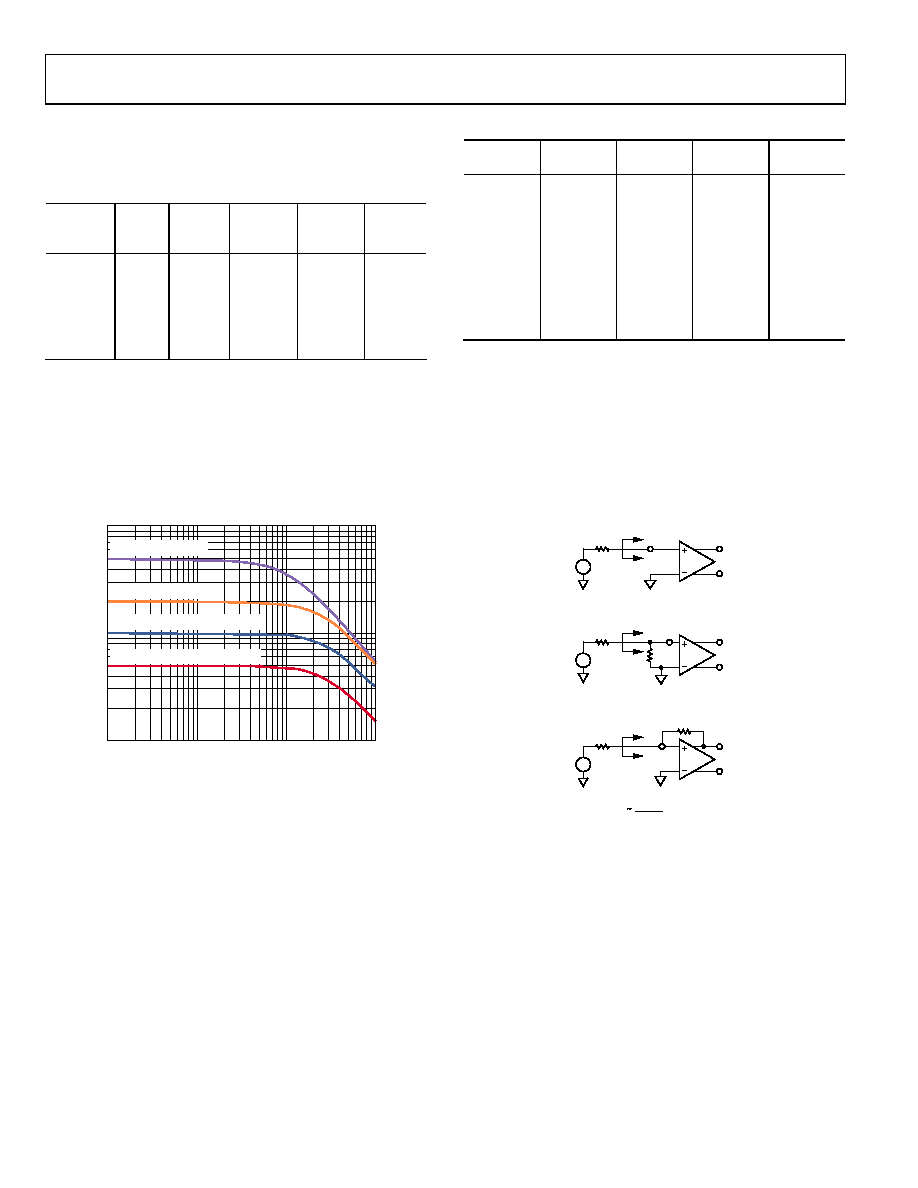
Figure 46. RIN vs. Frequency for Various Values of RFB
(Effects of RSH and CSH Are Also Shown)
Note that, at the lowest value of RIN (50 Ω), RIN peaks at frequencies
greater than 10 MHz. This is due to the BW roll-off of the LNA.
However, as can be seen for larger RIN values, parasitic capaci-
tance starts rolling off the signal BW before the LNA can produce
peaking. CSH further degrades the match; therefore, CSH should
not be used for values of RIN that are greater than 100 Ω.
of RIN.
CFB is needed in series with RFB because the dc levels at Pin LO-x
and Pin LI-x are unequal.
Table 10. Active Termination External Component Values
LNA Gain
(dB)
RIN (Ω)
RFB (Ω)
Minimum
CSH (pF)
BW (MHz)
15.6
50
200
90
57
17.9
50
250
70
69
21.3
50
350
50
88
15.6
100
400
30
57
17.9
100
500
20
69
21.3
100
700
10
88
15.6
200
800
N/A
72
17.9
200
1000
N/A
72
21.3
200
1400
N/A
72
LNA Noise
The short-circuit noise voltage (input-referred noise) is an
important limit on system performance. The short-circuit noise
voltage for the LNA is 0.75 nV/√Hz at a gain of 21.3 dB, including
the VGA noise at a VGA postamp gain of 27 dB. These measure-
ments, which were taken without a feedback resistor, provide
the basis for calculating the input noise and noise figure (NF)
performance of the configurations shown in Figure 47.
VOUT
UNTERMINATED
+
–
LI-x
RIN
RS
VOUT
SHUNT TERMINATION
+
–
LI-x
RIN
RS
VOUT
ACTIVE TERMINATION
+
–
LI-x
RIN
RFB
1 + A/2
RS
RIN =
09
42
3-
0
41
Figure 47. Input Configurations
results using these configurations and an input-referred noise
voltage of 2.5 nV/√Hz for the VGA. Unterminated (RFB = ∞)
operation exhibits the lowest equivalent input noise and noise
figure. Figure 49 shows the noise figure vs. source resistance
rising at low RS—where the LNA voltage noise is large compared
with the source noise—and at high RS due to the noise contribution
from RFB. The lowest NF is achieved when RS matches RIN.
相关PDF资料 |
PDF描述 |
|---|---|
| AD9393BBCZRL-80 | IC INTERFACE 80MHZ HDMI 76CSPBGA |
| AD9398KSTZ-150 | IC INTERFACE 150MHZ HDMI 100LQFP |
| AD9708ARU | IC DAC 8BIT 100MSPS 28-TSSOP |
| AD974BN | IC DAS 16BIT 4CH 200KSPS 28-DIP |
| AD9755ASTZRL | IC DAC 14BIT 300MSPS 48-LQFP |
相关代理商/技术参数 |
参数描述 |
|---|---|
| AD9279-BBCZ | 制造商:AD 制造商全称:Analog Devices 功能描述:Octal LNA/VGA/AAF/ADC and CW I/Q Demodulator |
| AD9280 | 制造商:AD 制造商全称:Analog Devices 功能描述:Complete 8-Bit, 32 MSPS, 95 mW CMOS A/D Converter |
| AD9280ARS | 功能描述:IC ADC CMOS 8BIT 32MSPS 28-SSOP RoHS:否 类别:集成电路 (IC) >> 数据采集 - 模数转换器 系列:- 产品培训模块:Lead (SnPb) Finish for COTS Obsolescence Mitigation Program 标准包装:2,500 系列:- 位数:12 采样率(每秒):3M 数据接口:- 转换器数目:- 功率耗散(最大):- 电压电源:- 工作温度:- 安装类型:表面贴装 封装/外壳:SOT-23-6 供应商设备封装:SOT-23-6 包装:带卷 (TR) 输入数目和类型:- |
| AD9280ARSRL | 功能描述:IC ADC 8BIT CMOS 32MSPS 28-SSOP RoHS:否 类别:集成电路 (IC) >> 数据采集 - 模数转换器 系列:- 产品培训模块:Lead (SnPb) Finish for COTS Obsolescence Mitigation Program 标准包装:2,500 系列:- 位数:12 采样率(每秒):3M 数据接口:- 转换器数目:- 功率耗散(最大):- 电压电源:- 工作温度:- 安装类型:表面贴装 封装/外壳:SOT-23-6 供应商设备封装:SOT-23-6 包装:带卷 (TR) 输入数目和类型:- |
| AD9280ARSZ | 功能描述:IC ADC CMOS 8BIT 32MSPS 28-SSOP RoHS:是 类别:集成电路 (IC) >> 数据采集 - 模数转换器 系列:- 标准包装:1 系列:microPOWER™ 位数:8 采样率(每秒):1M 数据接口:串行,SPI? 转换器数目:1 功率耗散(最大):- 电压电源:模拟和数字 工作温度:-40°C ~ 125°C 安装类型:表面贴装 封装/外壳:24-VFQFN 裸露焊盘 供应商设备封装:24-VQFN 裸露焊盘(4x4) 包装:Digi-Reel® 输入数目和类型:8 个单端,单极 产品目录页面:892 (CN2011-ZH PDF) 其它名称:296-25851-6 |
发布紧急采购,3分钟左右您将得到回复。