参数资料
| 型号: | AD9279BBCZ |
| 厂商: | Analog Devices Inc |
| 文件页数: | 20/44页 |
| 文件大小: | 0K |
| 描述: | IC ADC 12BIT 80MSPS 144CSPBGA |
| 标准包装: | 1 |
| 类型: | AAF,ADC,解调器,LNA,VGA |
| 分辨率(位): | 12 b |
| 采样率(每秒): | 80M |
| 数据接口: | 串行,SPI? |
| 电压电源: | 模拟和数字 |
| 电源电压: | 1.7 V ~ 1.9 V,2.7 V ~ 3.6 V |
| 工作温度: | -40°C ~ 85°C |
| 安装类型: | 表面贴装 |
| 封装/外壳: | 144-LFBGA,CSPBGA |
| 供应商设备封装: | 144-CSPBGA(10x10) |
| 包装: | 托盘 |
第1页第2页第3页第4页第5页第6页第7页第8页第9页第10页第11页第12页第13页第14页第15页第16页第17页第18页第19页当前第20页第21页第22页第23页第24页第25页第26页第27页第28页第29页第30页第31页第32页第33页第34页第35页第36页第37页第38页第39页第40页第41页第42页第43页第44页
AD9279
Rev. 0 | Page 27 of 44
Tuning is normally off to avoid changing the capacitor settings
during critical times. The tuning circuit is enabled through the
SPI. It is disabled automatically after 512 cycles of the ADC
sample clock. Initializing the tuning of the filter must be
performed after initial power-up and after reprogramming the
filter cutoff scaling or ADC sample rate.
A total of eight SPI-programmable settings allows the user to
vary the high-pass filter cutoff frequency as a function of the
low-pass cutoff frequency. Two examples are shown in Table 11:
one is for an 8 MHz low-pass cutoff frequency, and the other is
for an 18 MHz low-pass cutoff frequency. In both cases, as the
ratio decreases, the amount of rejection on the low-end fre-
quencies increases. Therefore, making the entire AAF frequency
pass band narrow can reduce low frequency noise or maximize
dynamic range for harmonic processing.
Table 11. SPI-Selectable High-Pass Filter Cutoff Options
High-Pass Cutoff Frequency
SPI Setting
Ratio1
Low-Pass
Cutoff = 8 MHz
Low-Pass
Cutoff = 18 MHz
0
12.00
670 kHz
1.5 MHz
1
8.57
930 kHz
2.1 MHz
2
6.67
1.2 MHz
2.7 MHz
3
5.46
1.47 MHz
3.3 MHz
4
4.62
1.73 MHz
3.9 MHz
5
4.00
2.0 MHz
4.5 MHz
6
3.53
2.27 MHz
5.1 MHz
7
3.16
2.53 MHz
5.7 MHz
1 Ratio = low-pass filter cutoff frequency/high-pass filter cutoff frequency.
ADC
The AD9279 uses a pipelined ADC architecture. The quantized
output from each stage is combined into a 12-bit result in the
digital correction logic. The pipelined architecture permits the
first stage to operate on a new input sample and the remaining
stages to operate on preceding samples. Sampling occurs on the
rising edge of the clock.
The output staging block aligns the data, corrects errors, and
passes the data to the output buffers. The data is then serialized
and aligned to the frame and output clocks.
Clock Input Considerations
For optimum performance, the AD9279 sample clock inputs
(CLK+ and CLK) should be clocked with a differential signal.
This signal is typically ac-coupled into the CLK+ and CLK pins
via a transformer or capacitors. These pins are biased internally
and require no additional bias.
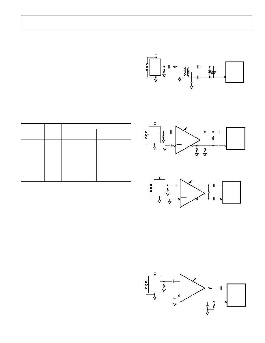
Figure 53 shows the preferred method for clocking the AD9279.
A low jitter clock source, such as the Valpey Fisher oscillator,
VFAC3-BHL-50 MHz, is converted from single-ended to differ-
ential using an RF transformer. The back-to-back Schottky
diodes across the secondary transformer limit clock excursions
into the AD9279 to approximately 0.8 V p-p differential. This
helps to prevent the large voltage swings of the clock from
feeding through to other portions of the AD9279, and it
preserves the fast rise and fall times of the signal, which are
critical to low jitter performance.
0.1F
SCHOTTKY
DIODES:
HSM2812
3.3V
50
100
CLK–
CLK+
AD9279
MINI-CIRCUITS
ADT1-1WT, 1:1Z
XFMR
VFAC3
OUT
0
94
23
-05
5
Figure 53. Transformer-Coupled Differential Clock
If a low jitter clock is available, another option is to ac-couple
a differential PECL signal to the sample clock input pins, as
shown in Figure 54. The AD951x family of clock drivers offers
excellent jitter performance.
100
0.1F
240
240
AD951x FAMILY
CLK
*50
RESISTOR IS OPTIONAL.
PECL DRIVER
3.3V
OUT
VFAC3
09
42
3-
0
56
CLK–
CLK+
AD9279
50
*
Figure 54. Differential PECL Sample Clock
100
0.1F
AD951x FAMILY
CLK
*50
RESISTOR IS OPTIONAL.
LVDS DRIVER
3.3V
OUT
VFAC3
09
42
3-
0
57
CLK–
CLK+
AD9279
50
*
Figure 55. Differential LVDS Sample Clock
In some applications, it is acceptable to drive the sample clock
inputs with a single-ended CMOS signal. In such applications,
CLK+ should be driven directly from a CMOS gate, and the
CLK pin should be bypassed to ground with a 0.1 μF capacitor
in parallel with a 39 kΩ resistor (see Figure 56). Although the
CLK+ input circuit supply is AVDD1 (1.8 V), this input is
designed to withstand input voltages of up to 3.3 V, making the
selection of the drive logic voltage very flexible.
0.1F
OPTIONAL
100
0.1F
39k
CMOS DRIVER
0.1F
CLK
*50
RESISTOR IS OPTIONAL.
AD951x FAMILY
3.3V
OUT
VFAC3
09
42
3-
05
8
CLK–
CLK+
AD9279
50
*
Figure 56. Single-Ended 1.8 V CMOS Sample Clock
相关PDF资料 |
PDF描述 |
|---|---|
| AD9393BBCZRL-80 | IC INTERFACE 80MHZ HDMI 76CSPBGA |
| AD9398KSTZ-150 | IC INTERFACE 150MHZ HDMI 100LQFP |
| AD9708ARU | IC DAC 8BIT 100MSPS 28-TSSOP |
| AD974BN | IC DAS 16BIT 4CH 200KSPS 28-DIP |
| AD9755ASTZRL | IC DAC 14BIT 300MSPS 48-LQFP |
相关代理商/技术参数 |
参数描述 |
|---|---|
| AD9279-BBCZ | 制造商:AD 制造商全称:Analog Devices 功能描述:Octal LNA/VGA/AAF/ADC and CW I/Q Demodulator |
| AD9280 | 制造商:AD 制造商全称:Analog Devices 功能描述:Complete 8-Bit, 32 MSPS, 95 mW CMOS A/D Converter |
| AD9280ARS | 功能描述:IC ADC CMOS 8BIT 32MSPS 28-SSOP RoHS:否 类别:集成电路 (IC) >> 数据采集 - 模数转换器 系列:- 产品培训模块:Lead (SnPb) Finish for COTS Obsolescence Mitigation Program 标准包装:2,500 系列:- 位数:12 采样率(每秒):3M 数据接口:- 转换器数目:- 功率耗散(最大):- 电压电源:- 工作温度:- 安装类型:表面贴装 封装/外壳:SOT-23-6 供应商设备封装:SOT-23-6 包装:带卷 (TR) 输入数目和类型:- |
| AD9280ARSRL | 功能描述:IC ADC 8BIT CMOS 32MSPS 28-SSOP RoHS:否 类别:集成电路 (IC) >> 数据采集 - 模数转换器 系列:- 产品培训模块:Lead (SnPb) Finish for COTS Obsolescence Mitigation Program 标准包装:2,500 系列:- 位数:12 采样率(每秒):3M 数据接口:- 转换器数目:- 功率耗散(最大):- 电压电源:- 工作温度:- 安装类型:表面贴装 封装/外壳:SOT-23-6 供应商设备封装:SOT-23-6 包装:带卷 (TR) 输入数目和类型:- |
| AD9280ARSZ | 功能描述:IC ADC CMOS 8BIT 32MSPS 28-SSOP RoHS:是 类别:集成电路 (IC) >> 数据采集 - 模数转换器 系列:- 标准包装:1 系列:microPOWER™ 位数:8 采样率(每秒):1M 数据接口:串行,SPI? 转换器数目:1 功率耗散(最大):- 电压电源:模拟和数字 工作温度:-40°C ~ 125°C 安装类型:表面贴装 封装/外壳:24-VFQFN 裸露焊盘 供应商设备封装:24-VQFN 裸露焊盘(4x4) 包装:Digi-Reel® 输入数目和类型:8 个单端,单极 产品目录页面:892 (CN2011-ZH PDF) 其它名称:296-25851-6 |
发布紧急采购,3分钟左右您将得到回复。