参数资料
| 型号: | AD9279BBCZ |
| 厂商: | Analog Devices Inc |
| 文件页数: | 21/44页 |
| 文件大小: | 0K |
| 描述: | IC ADC 12BIT 80MSPS 144CSPBGA |
| 标准包装: | 1 |
| 类型: | AAF,ADC,解调器,LNA,VGA |
| 分辨率(位): | 12 b |
| 采样率(每秒): | 80M |
| 数据接口: | 串行,SPI? |
| 电压电源: | 模拟和数字 |
| 电源电压: | 1.7 V ~ 1.9 V,2.7 V ~ 3.6 V |
| 工作温度: | -40°C ~ 85°C |
| 安装类型: | 表面贴装 |
| 封装/外壳: | 144-LFBGA,CSPBGA |
| 供应商设备封装: | 144-CSPBGA(10x10) |
| 包装: | 托盘 |
第1页第2页第3页第4页第5页第6页第7页第8页第9页第10页第11页第12页第13页第14页第15页第16页第17页第18页第19页第20页当前第21页第22页第23页第24页第25页第26页第27页第28页第29页第30页第31页第32页第33页第34页第35页第36页第37页第38页第39页第40页第41页第42页第43页第44页
AD9279
Rev. 0 | Page 28 of 44
0.1F
CMOS DRIVER
OPTIONAL
100
0.1F
CLK
*50
RESISTOR IS OPTIONAL.
AD951x FAMILY
3.3V
OUT
VFAC3
09
42
3-
0
59
CLK–
CLK+
AD9279
50
*
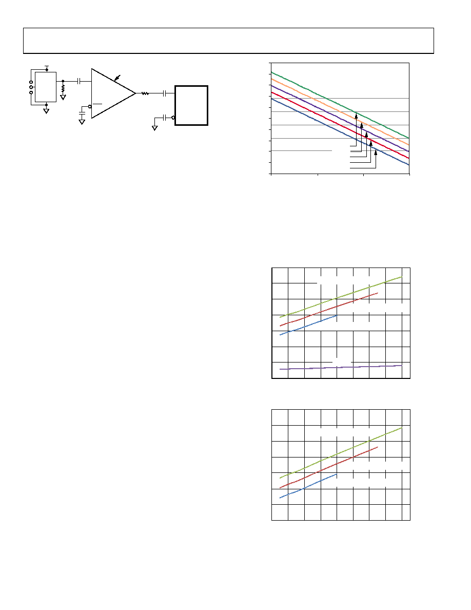
Figure 57. Single-Ended 3.3 V CMOS Sample Clock
Clock Duty Cycle Considerations
Typical high speed ADCs use both clock edges to generate a
variety of internal timing signals. As a result, these ADCs may
be sensitive to the clock duty cycle. Commonly, a 5% tolerance is
required on the clock duty cycle to maintain dynamic performance
characteristics. The AD9279 contains a duty cycle stabilizer (DCS)
that retimes the nonsampling edge, providing an internal clock
signal with a nominal 50% duty cycle. This allows a wide range
of clock input duty cycles without affecting the performance of
the AD9279. When the DCS is on, noise and distortion perfor-
mance are nearly flat for a wide range of duty cycles. However,
some applications may require the DCS function to be off. If so,
keep in mind that the dynamic range performance can be affected
when operated in this mode. See Table 19 for more details on
using this feature.
The duty cycle stabilizer uses a delay-locked loop (DLL) to
create the nonsampling edge. As a result, any changes to the
sampling frequency require approximately eight clock cycles
to allow the DLL to acquire and lock to the new rate.
Clock Jitter Considerations
High speed, high resolution ADCs are sensitive to the quality of the
clock input. The degradation in SNR at a given input frequency (fA)
due only to aperture jitter (tJ) can be calculated as follows:
SNR Degradation = 20 × log 10(1/2 × π × fA × tJ)
In this equation, the rms aperture jitter represents the root mean
square of all jitter sources, including the clock input, analog input
signal, and ADC aperture jitter. IF undersampling applications
are particularly sensitive to jitter (see Figure 58).
The clock input should be treated as an analog signal in cases
where aperture jitter may affect the dynamic range of the AD9279.
Power supplies for clock drivers should be separated from the
ADC output driver supplies to avoid modulating the clock signal
with digital noise. Low jitter, crystal-controlled oscillators make
the best clock sources, such as the Valpey Fisher VFAC3 series.
If the clock is generated from another type of source (by gating,
dividing, or other methods), it should be retimed by the original
clock during the last step.
Refer to the AN-501 Application Note and the AN-756
Application Note for more in-depth information about how
jitter performance relates to ADCs (visit www.analog.com).
1
10
100
1000
16 BITS
14 BITS
12 BITS
30
40
50
60
70
80
90
100
110
120
130
0.125ps
0.5ps
1.0ps
2.0ps
ANALOG INPUT FREQUENCY (MHz)
10 BITS
8 BITS
RMS CLOCK JITTER REQUIREMENT
S
NR
(
d
B
)
09
42
3-
06
0
0.25ps
Figure 58. Ideal SNR vs. Input Frequency and Jitter
Power Dissipation and Power-Down Mode
As shown in Figure 59 and Figure 60, the power dissipated by
the AD9279 is proportional to its sample rate. The digital power
dissipation does not vary significantly because it is determined
primarily by the DRVDD supply and the bias current of the
LVDS output drivers.
350
300
250
200
150
100
50
0
1020
30
40
50
60
7080
SAMPLING FREQUENCY (MSPS)
CU
RRE
N
T
S
(
m
A
)
09
42
3-
06
1
MODE III,
fSAMPLE = 80MSPS
IDRVDD
MODE II,
fSAMPLE = 65MSPS
MODE I,
fSAMPLE = 40MSPS
Figure 59. Supply Current vs. fSAMPLE for fIN = 5 MHz
180
170
160
150
140
130
120
110
0
1020
30
40
50
60
7080
SAMPLING FREQUENCY (MSPS)
P
O
W
E
R/
CHANN
E
L
(
m
W
/C
H)
09
42
3-
06
2
MODE III,
fSAMPLE = 80MSPS
MODE II,
fSAMPLE = 65MSPS
MODE I,
fSAMPLE = 40MSPS
Figure 60. Power per Channel vs. fSAMPLE for fIN = 5 MHz
The AD9279 features scalable LNA bias currents (see Table 19,
Register 0x12). The default LNA bias current settings are high.
相关PDF资料 |
PDF描述 |
|---|---|
| AD9393BBCZRL-80 | IC INTERFACE 80MHZ HDMI 76CSPBGA |
| AD9398KSTZ-150 | IC INTERFACE 150MHZ HDMI 100LQFP |
| AD9708ARU | IC DAC 8BIT 100MSPS 28-TSSOP |
| AD974BN | IC DAS 16BIT 4CH 200KSPS 28-DIP |
| AD9755ASTZRL | IC DAC 14BIT 300MSPS 48-LQFP |
相关代理商/技术参数 |
参数描述 |
|---|---|
| AD9279-BBCZ | 制造商:AD 制造商全称:Analog Devices 功能描述:Octal LNA/VGA/AAF/ADC and CW I/Q Demodulator |
| AD9280 | 制造商:AD 制造商全称:Analog Devices 功能描述:Complete 8-Bit, 32 MSPS, 95 mW CMOS A/D Converter |
| AD9280ARS | 功能描述:IC ADC CMOS 8BIT 32MSPS 28-SSOP RoHS:否 类别:集成电路 (IC) >> 数据采集 - 模数转换器 系列:- 产品培训模块:Lead (SnPb) Finish for COTS Obsolescence Mitigation Program 标准包装:2,500 系列:- 位数:12 采样率(每秒):3M 数据接口:- 转换器数目:- 功率耗散(最大):- 电压电源:- 工作温度:- 安装类型:表面贴装 封装/外壳:SOT-23-6 供应商设备封装:SOT-23-6 包装:带卷 (TR) 输入数目和类型:- |
| AD9280ARSRL | 功能描述:IC ADC 8BIT CMOS 32MSPS 28-SSOP RoHS:否 类别:集成电路 (IC) >> 数据采集 - 模数转换器 系列:- 产品培训模块:Lead (SnPb) Finish for COTS Obsolescence Mitigation Program 标准包装:2,500 系列:- 位数:12 采样率(每秒):3M 数据接口:- 转换器数目:- 功率耗散(最大):- 电压电源:- 工作温度:- 安装类型:表面贴装 封装/外壳:SOT-23-6 供应商设备封装:SOT-23-6 包装:带卷 (TR) 输入数目和类型:- |
| AD9280ARSZ | 功能描述:IC ADC CMOS 8BIT 32MSPS 28-SSOP RoHS:是 类别:集成电路 (IC) >> 数据采集 - 模数转换器 系列:- 标准包装:1 系列:microPOWER™ 位数:8 采样率(每秒):1M 数据接口:串行,SPI? 转换器数目:1 功率耗散(最大):- 电压电源:模拟和数字 工作温度:-40°C ~ 125°C 安装类型:表面贴装 封装/外壳:24-VFQFN 裸露焊盘 供应商设备封装:24-VQFN 裸露焊盘(4x4) 包装:Digi-Reel® 输入数目和类型:8 个单端,单极 产品目录页面:892 (CN2011-ZH PDF) 其它名称:296-25851-6 |
发布紧急采购,3分钟左右您将得到回复。