参数资料
| 型号: | AD9512BCPZ |
| 厂商: | Analog Devices Inc |
| 文件页数: | 17/48页 |
| 文件大小: | 0K |
| 描述: | IC CLOCK DIST 5OUT PLL 48LFCSP |
| 标准包装: | 1 |
| 类型: | 扇出缓冲器(分配),除法器 |
| PLL: | 无 |
| 输入: | 时钟 |
| 输出: | CMOS,LVDS,LVPECL |
| 电路数: | 1 |
| 比率 - 输入:输出: | 2:5 |
| 差分 - 输入:输出: | 是/是 |
| 频率 - 最大: | 1.2GHz |
| 除法器/乘法器: | 是/无 |
| 电源电压: | 3.135 V ~ 3.465 V |
| 工作温度: | -40°C ~ 85°C |
| 安装类型: | 表面贴装 |
| 封装/外壳: | 48-VFQFN 裸露焊盘,CSP |
| 供应商设备封装: | 48-LFCSP-VQ(7x7) |
| 包装: | 托盘 |
第1页第2页第3页第4页第5页第6页第7页第8页第9页第10页第11页第12页第13页第14页第15页第16页当前第17页第18页第19页第20页第21页第22页第23页第24页第25页第26页第27页第28页第29页第30页第31页第32页第33页第34页第35页第36页第37页第38页第39页第40页第41页第42页第43页第44页第45页第46页第47页第48页
AD9512
Rev. A | Page 24 of 48
FUNCTIONAL DESCRIPTION
OVERALL
Figure 23 shows a block diagram of the AD9512. The AD9512
accepts inputs on either of two clock inputs (CLK1 or CLK2).
This clock can be divided by any integer value from 1 to 32.
The duty cycle and relative phase of the outputs can be selected.
There are three LVPECL outputs (OUT0, OUT1, OUT2) and
two outputs that can be either LVDS or CMOS level outputs
(OUT3, OUT4). OUT4 can also make use of a variable
delay block.
The AD9512 provides clock distribution function only; there is
no clock clean-up. The jitter of the input clock signal is passed
along directly to the distribution section and can dominate at
the clock outputs.
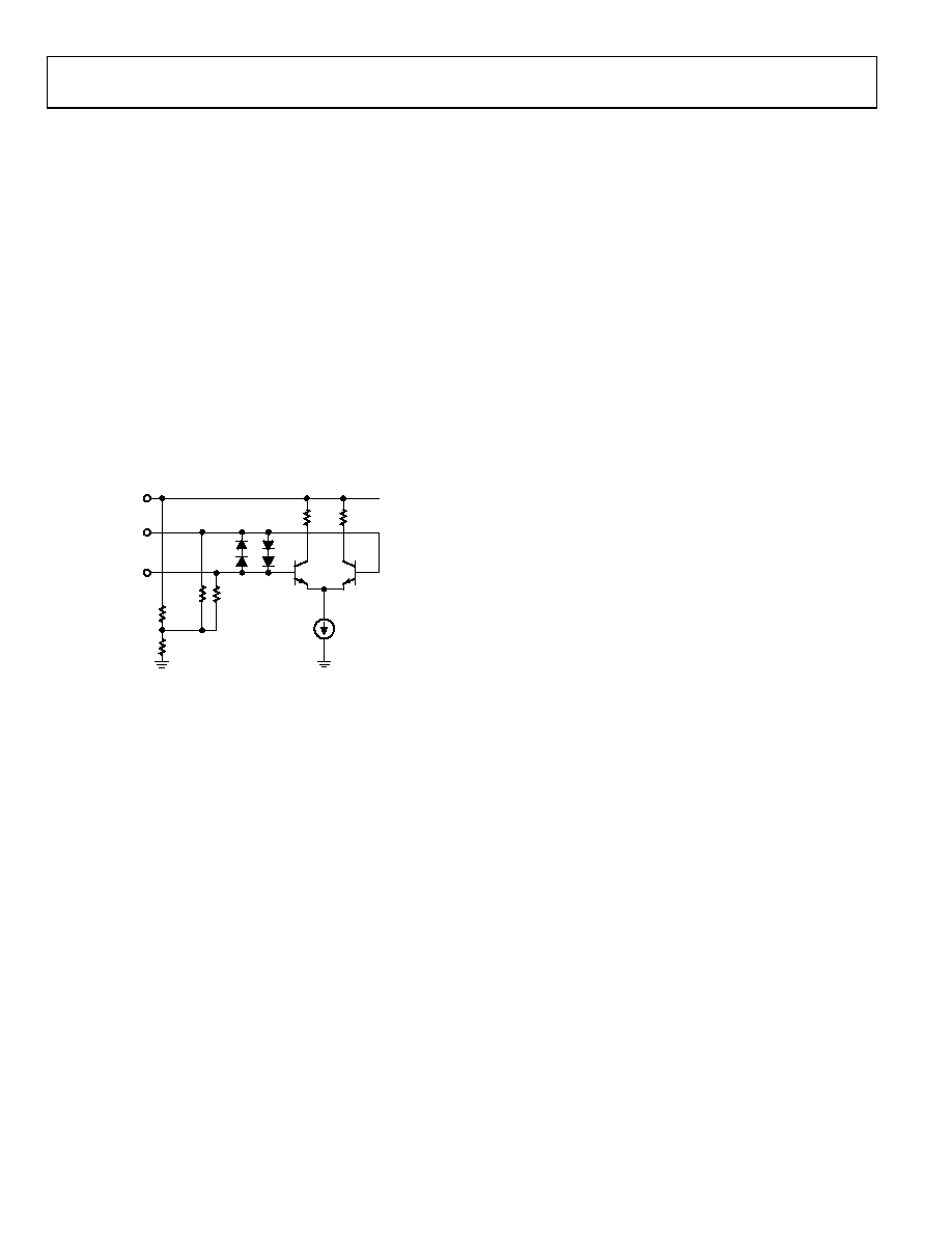
See Figure 24 for the equivalent circuit of CLK1 and CLK2.
05287-
016
VS
CLOCK INPUT
STAGE
CLK
CLKB
5k
Ω
5k
Ω
2.5k
Ω
2.5k
Ω
Figure 24. CLK1, CLK2 Equivalent Input Circuit
FUNCTION PIN
The FUNCTION pin (Pin 12) has three functions that are
selected by the value in Register 58h<6:5>. There is an internal
30 kΩ pull-down resistor on this pin.
RESETB: 58h<6:5> = 00b (Default)
In its default mode, the FUNCTION pin acts as RESETB, which
generates an asynchronous reset or hard reset when pulled low.
The resulting reset writes the default values into the serial
control port buffer registers as well as loading them into the
chip control registers. The AD9512 immediately resumes
operation according to the default values. When the pin is taken
high again, an asynchronous sync is issued (see the SYNCB:
58h<6:5> = 01b section).
SYNCB: 58h<6:5> = 01b
The FUNCTION pin can be used to cause a synchronization
or alignment of phase among the various clock outputs.
The synchronization applies only to clock outputs that:
are not powered down
the divider is not masked (no sync = 0)
are not bypassed (bypass = 0)
SYNCB is level and rising edge sensitive. When SYNCB is low,
the set of affected outputs are held in a predetermined state,
defined by each divider’s start high bit. On a rising edge, the
dividers begin after a predefined number of fast clock cycles
(fast clock is the selected clock input, CLK1 or CLK2) as
determined by the values in the divider’s phase offset bits.
The SYNCB application of the FUNCTION pin is always active,
regardless of whether the pin is also assigned to perform reset
or power-down. When the SYNCB function is selected, the
FUNCTION pin does not act as either RESETB or PDB.
PDB: 58h<6:5> = 11b
The FUNCTION pin can also be programmed to work as an
asynchronous full power-down, PDB. Even in this full power-
down mode, there is still some residual VS current because
some on-chip references continue to operate. In PDB mode, the
FUNCTION pin is active low. The chip remains in a power-
down state until PDB is returned to logic high. The chip returns
to the settings programmed prior to the power-down.
See the Chip Power-Down or Sleep Mode—PDB section for more
details on what occurs during a PDB initiated power-down.
DSYNC AND DSYNCB PINS
The DSYNC and DSYNCB pins (Pin 1 and Pin 2) are used
when the AD9512 is used in a multichip synchronized
configuration (see the Multichip Synchronization section).
CLOCK INPUTS
Two clock inputs (CLK1, CLK2) are available for use on the
AD9512. CLK1 and CLK2 can accept inputs up to 1600 MHz.
See Figure 24 for the CLK1 and CLK2 equivalent input circuit.
The clock inputs are fully differential and self-biased. The signal
should be ac-coupled using capacitors. If a single-ended input
must be used, this can be accommodated by ac coupling to one
side of the differential input only. The other side of the input
should be bypassed to a quiet ac ground by a capacitor.
The unselected clock input (either CLK1 or CLK2) should be
powered down to eliminate any possibility of unwanted
crosstalk between the selected clock input and the unselected
clock input.
相关PDF资料 |
PDF描述 |
|---|---|
| V28A36H200BF2 | CONVERTER MOD DC/DC 36V 200W |
| V28A28H200BL3 | CONVERTER MOD DC/DC 28V 200W |
| V28A28H200BG2 | CONVERTER MOD DC/DC 28V 200W |
| V28A28H200B2 | CONVERTER MOD DC/DC 28V 200W |
| V28A24H200BL2 | CONVERTER MOD DC/DC 24V 200W |
相关代理商/技术参数 |
参数描述 |
|---|---|
| AD9512BCPZ-REEL7 | 功能描述:IC CLOCK DIST 5OUT PLL 48LFCSP RoHS:是 类别:集成电路 (IC) >> 时钟/计时 - 时钟发生器,PLL,频率合成器 系列:- 标准包装:2,000 系列:- 类型:PLL 时钟发生器 PLL:带旁路 输入:LVCMOS,LVPECL 输出:LVCMOS 电路数:1 比率 - 输入:输出:2:11 差分 - 输入:输出:是/无 频率 - 最大:240MHz 除法器/乘法器:是/无 电源电压:3.135 V ~ 3.465 V 工作温度:0°C ~ 70°C 安装类型:表面贴装 封装/外壳:32-LQFP 供应商设备封装:32-TQFP(7x7) 包装:带卷 (TR) |
| AD9512-EP | 制造商:AD 制造商全称:Analog Devices 功能描述:1.2 GHz Clock Distribution IC, 1.6 GHz Inputs, Dividers, Five Outputs |
| AD9512-PCB | 制造商:AD 制造商全称:Analog Devices 功能描述:1.2 GHz Clock Distribution IC, 1.6 GHz Inputs, Dividers, Delay Adjust, Five Outputs |
| AD9512UCPZ-EP | 功能描述:IC CLOCK DIST 5OUT PLL 48LFCSP RoHS:是 类别:集成电路 (IC) >> 时钟/计时 - 时钟发生器,PLL,频率合成器 系列:- 标准包装:2,000 系列:- 类型:PLL 时钟发生器 PLL:带旁路 输入:LVCMOS,LVPECL 输出:LVCMOS 电路数:1 比率 - 输入:输出:2:11 差分 - 输入:输出:是/无 频率 - 最大:240MHz 除法器/乘法器:是/无 电源电压:3.135 V ~ 3.465 V 工作温度:0°C ~ 70°C 安装类型:表面贴装 封装/外壳:32-LQFP 供应商设备封装:32-TQFP(7x7) 包装:带卷 (TR) |
| AD9512UCPZ-EP-R7 | 功能描述:IC CLOCK DIST 5OUT PLL 48LFCSP RoHS:是 类别:集成电路 (IC) >> 时钟/计时 - 时钟发生器,PLL,频率合成器 系列:- 标准包装:2,000 系列:- 类型:PLL 时钟发生器 PLL:带旁路 输入:LVCMOS,LVPECL 输出:LVCMOS 电路数:1 比率 - 输入:输出:2:11 差分 - 输入:输出:是/无 频率 - 最大:240MHz 除法器/乘法器:是/无 电源电压:3.135 V ~ 3.465 V 工作温度:0°C ~ 70°C 安装类型:表面贴装 封装/外壳:32-LQFP 供应商设备封装:32-TQFP(7x7) 包装:带卷 (TR) |
发布紧急采购,3分钟左右您将得到回复。