- 您现在的位置:买卖IC网 > PDF目录16849 > AD9515/PCBZ (Analog Devices Inc)BOARD EVAL CLOCK 2CH AD9515 PDF资料下载
参数资料
| 型号: | AD9515/PCBZ |
| 厂商: | Analog Devices Inc |
| 文件页数: | 19/28页 |
| 文件大小: | 0K |
| 描述: | BOARD EVAL CLOCK 2CH AD9515 |
| 设计资源: | Low Jitter Sampling Clock Generator for High Performance ADCs Using AD9958/9858 and AD9515 (CN0109) AD9513/14/15 Eval Brd Schematics AD9513/14/15 Gerber Files AD9515 Eval Brd BOM |
| 标准包装: | 1 |
| 主要目的: | 计时,时钟分配 |
| 已用 IC / 零件: | AD9515 |
| 已供物品: | 板 |
| 相关产品: | AD9515BCPZ-ND - IC CLOCK DIST 2OUT PLL 32LFCSP AD9515BCPZ-REEL7-ND - IC CLOCK DIST 2OUT PLL 32LFCSP |
第1页第2页第3页第4页第5页第6页第7页第8页第9页第10页第11页第12页第13页第14页第15页第16页第17页第18页当前第19页第20页第21页第22页第23页第24页第25页第26页第27页第28页
AD9515
Data Sheet
Rev. A | Page 26 of 28
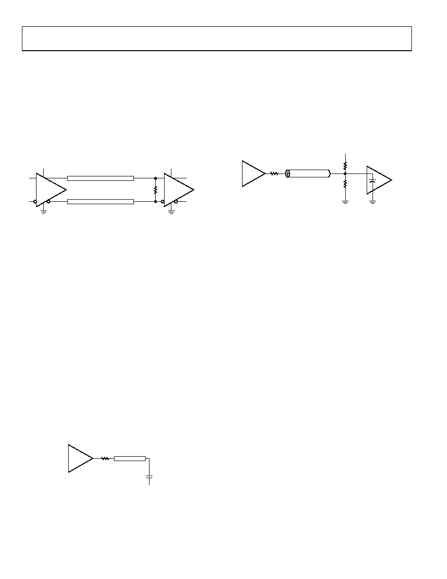
LVDS CLOCK DISTRIBUTION
The AD9515 provides one clock output (OUT2) that is
selectable as either CMOS or LVDS levels. Low voltage
differential signaling (LVDS) is a differential output option
for OUT2. LVDS uses a current mode output stage. The
current is 3.5 mA, which yields 350 mV output swing across
a 100 resistor. The LVDS output meets or exceeds all
ANSI/TIA/EIA-644 specifications.
A recommended termination circuit for the LVDS outputs
is shown in Figure 38.
VS
LVDS
100
DIFFERENTIAL (COUPLED)
VS
LVDS
100
05597-032
Figure 38. LVDS Output Termination
See Application Note AN-586 at www.analog.com for more
information on LVDS.
CMOS CLOCK DISTRIBUTION
The AD9515 provides one output (OUT1) that is selectable as
either CMOS or LVDS levels. When selected as CMOS, this
output provides for driving devices requiring CMOS level logic
at their clock inputs.
Whenever single-ended CMOS clocking is used, some of the
following general guidelines should be used.
Point-to-point nets should be designed such that a driver has
only one receiver on the net, if possible. This allows for simple
termination schemes and minimizes ringing due to possible
mismatched impedances on the net. Series termination at the
source is generally required to provide transmission line
matching and/or to reduce current transients at the driver. The
value of the resistor is dependent on the board design and
timing requirements (typically 10 to 100 is used). CMOS
outputs are also limited in terms of the capacitive load or trace
length that they can drive. Typically, trace lengths less than
3 inches are recommended to preserve signal rise/fall times and
preserve signal integrity.
10
MICROSTRIP
GND
5pF
60.4
1.0 INCH
CMOS
05597-033
Figure 39. Series Termination of CMOS Output
Termination at the far end of the PCB trace is a second option.
The CMOS outputs of the AD9515 do not supply enough
current to provide a full voltage swing with a low impedance
resistive, far-end termination, as shown in Figure 40. The
far-end termination network should match the PCB trace
impedance and provide the desired switching point. The
reduced signal swing may still meet receiver input requirements
in some applications. This can be useful when driving long
trace lengths on less critical nets.
50
10
OUT1/OUT1B
SELECTED AS CMOS
VS
CMOS
3pF
100
100
05597-034
Figure 40. CMOS Output with Far-End Termination
Because of the limitations of single-ended CMOS clocking,
consider using differential outputs when driving high speed
signals over long traces. The AD9515 offers both LVPECL and
LVDS outputs that are better suited for driving long traces
where the inherent noise immunity of differential signaling
provides superior performance for clocking converters.
SETUP PINS (S0 TO S10)
The setup pins that require a logic level of VS (internal self-
bias) should be tied together and bypassed to ground via a
capacitor.
The setup pins that require a logic level of VS should be tied
together, along with the VREF pin, and bypassed to ground via
a capacitor.
POWER AND GROUNDING CONSIDERATIONS AND
POWER SUPPLY REJECTION
Many applications seek high speed and performance under less
than ideal operating conditions. In these application circuits, the
implementation and construction of the PCB is as important
as the circuit design. Proper RF techniques must be used for
device selection, placement, and routing, as well as power
supply bypassing and grounding to ensure optimum
performance.
相关PDF资料 |
PDF描述 |
|---|---|
| ECC30DCAN | CONN EDGECARD 60POS R/A .100 SLD |
| ECC30DCAH | CONN EDGECARD 60POS R/A .100 SLD |
| AD9510-VCO/PCBZ | BOARD EVALUATION FOR AD9510 |
| RBM22DSUI | CONN EDGECARD 44POS DIP .156 SLD |
| A2MXS-2406M | ADM24S/AE24M/X |
相关代理商/技术参数 |
参数描述 |
|---|---|
| AD95160 | 制造商:AD 制造商全称:Analog Devices 功能描述:14-Channel Clock Generator with Integrated 2.8 GHz VCO |
| AD9516-0 | 制造商:AD 制造商全称:Analog Devices 功能描述:14-Output Clock Generator with Integrated 2.8 GHz VCO |
| AD9516-0/PCBZ | 功能描述:IC CLOCK GEN 2.8GHZ VCO 64-LFCSP RoHS:是 类别:编程器,开发系统 >> 评估演示板和套件 系列:- 标准包装:1 系列:- 主要目的:电信,线路接口单元(LIU) 嵌入式:- 已用 IC / 零件:IDT82V2081 主要属性:T1/J1/E1 LIU 次要属性:- 已供物品:板,电源,线缆,CD 其它名称:82EBV2081 |
| AD9516-0_07 | 制造商:AD 制造商全称:Analog Devices 功能描述:14-Output Clock Generator with Integrated 2.8 GHz VCO |
| AD9516-0BCPZ | 功能描述:IC CLOCK GEN 2.8GHZ VCO 64-LFCSP RoHS:是 类别:集成电路 (IC) >> 时钟/计时 - 时钟发生器,PLL,频率合成器 系列:- 标准包装:2,000 系列:- 类型:PLL 时钟发生器 PLL:带旁路 输入:LVCMOS,LVPECL 输出:LVCMOS 电路数:1 比率 - 输入:输出:2:11 差分 - 输入:输出:是/无 频率 - 最大:240MHz 除法器/乘法器:是/无 电源电压:3.135 V ~ 3.465 V 工作温度:0°C ~ 70°C 安装类型:表面贴装 封装/外壳:32-LQFP 供应商设备封装:32-TQFP(7x7) 包装:带卷 (TR) |
发布紧急采购,3分钟左右您将得到回复。