- 您现在的位置:买卖IC网 > PDF目录9663 > AD9523BCPZ-REEL7 (Analog Devices Inc)IC INTEGER-N CLCK GEN 72LFCSP PDF资料下载
参数资料
| 型号: | AD9523BCPZ-REEL7 |
| 厂商: | Analog Devices Inc |
| 文件页数: | 18/60页 |
| 文件大小: | 0K |
| 描述: | IC INTEGER-N CLCK GEN 72LFCSP |
| 标准包装: | 400 |
| 类型: | 时钟/频率发生器,扇出缓冲器(分配) |
| PLL: | 是 |
| 主要目的: | 以太网,光纤通道,SONET/SDH |
| 输入: | CMOS |
| 输出: | HSTL,LVCMOS,LVDS,LVPECL |
| 电路数: | 1 |
| 比率 - 输入:输出: | 2:14 |
| 差分 - 输入:输出: | 是/是 |
| 频率 - 最大: | 1GHz |
| 电源电压: | 1.71 V ~ 3.465 V |
| 工作温度: | -40°C ~ 85°C |
| 安装类型: | 表面贴装 |
| 封装/外壳: | 72-VFQFN 裸露焊盘,CSP |
| 供应商设备封装: | 72-LFCSP-VQ(10x10) |
| 包装: | 带卷 (TR) |
| 配用: | AD9523/PCBZ-ND - BOARD EVAL FOR AD9523 |
第1页第2页第3页第4页第5页第6页第7页第8页第9页第10页第11页第12页第13页第14页第15页第16页第17页当前第18页第19页第20页第21页第22页第23页第24页第25页第26页第27页第28页第29页第30页第31页第32页第33页第34页第35页第36页第37页第38页第39页第40页第41页第42页第43页第44页第45页第46页第47页第48页第49页第50页第51页第52页第53页第54页第55页第56页第57页第58页第59页第60页
Data Sheet
AD9523
Rev. C | Page 25 of 60
When using the sync dividers bit, the user first sets and then
clears the bit. The synchronization event is the clearing
operation (that is, the Logic 1 to Logic 0 transition of the bit).
The dividers are all automatically synchronized to each other
when PLL2 is ready. The dividers support programmable phase
offsets from 0 to 63 steps, in half periods of the input clock (for
example, the VCO divider output clock). The phase offsets are
incorporated in the dividers through a preset for the first output
clock period of each divider. Phase offsets are sup-ported only by
programming the initial phase and divide value and then issuing a
sync to the distribution (automatically at startup or manually, if
desired).
When using the SYNC pin (Pin 17), there are 11 VCO divider
output pipe line delays plus one period of the clock from the
rising edge of SYNC to the clock output. There is at least one
extra VCO divider period of uncertainty because the SYNC
signal and the VCO divider output are asynchronous.
In normal operation, the phase offsets are already programmed
through the EEPROM or the SPI/I2C port before the AD9523
starts to provide outputs. Although the user cannot adjust the
phase offsets while the dividers are operating, it is possible to
adjust the phase of all the outputs together without powering
down PLL1 and PLL2. This is accomplished by programming
the new phase offset, using Bits[7:2] in Register 0x192 (see
Table 51) and then issuing a divide sync signal by using the
SYNC pin or the sync dividers bit (Register 0x232, Bit 0). All
outputs that are not programmed to ignore the sync are disabled
temporarily while the sync is active. Note that, if an output is used
for the zero delay path, it also disappears momentarily. However,
this is desirable because it ensures that all the synchronized outputs
have a deterministic phase relationship with respect to the zero
delay output and, therefore, also with respect to the input.
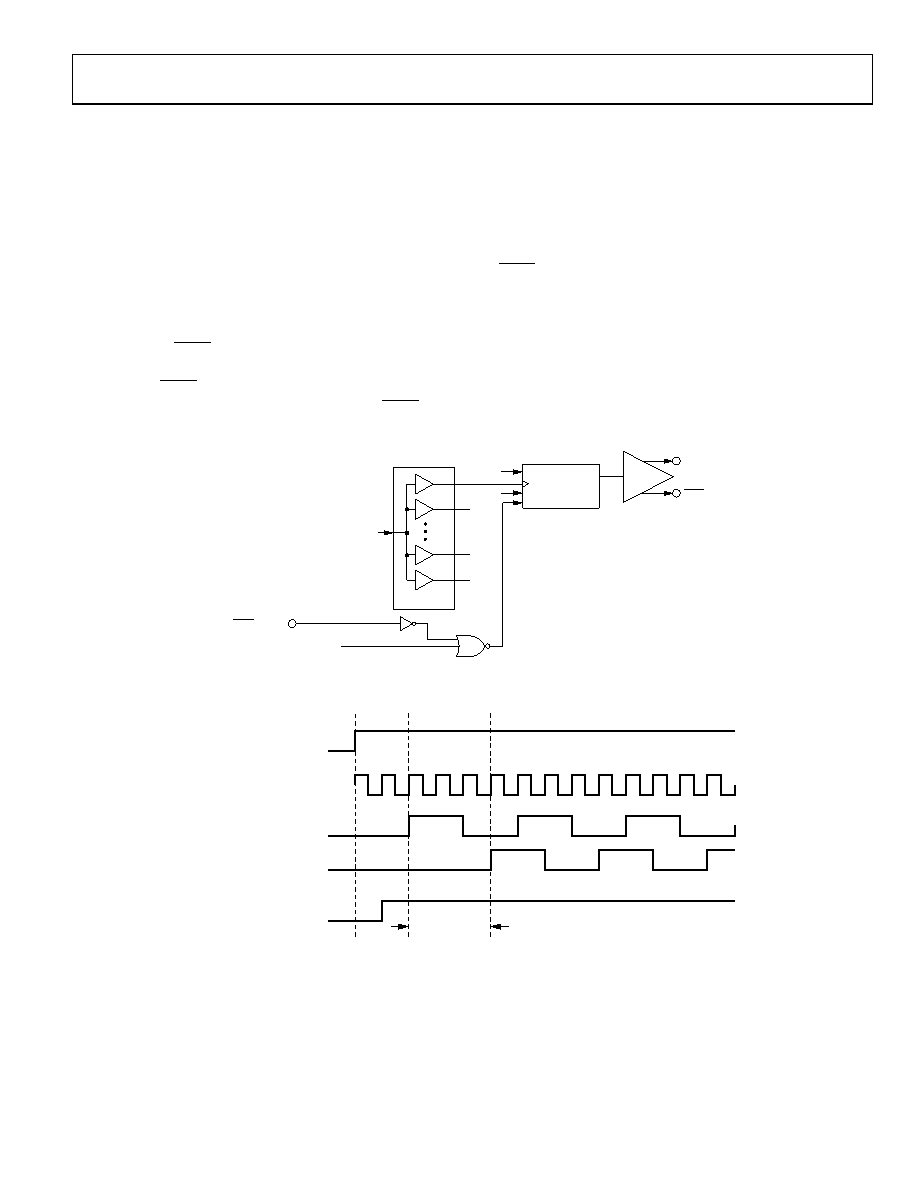
FAN OUT
VCO OUTPUT DIVIDER
SYNC (PIN 17)
SYNC
SYNC DIVIDERS BIT
08439-
02
5
DIVIDER
DRIVER
OUTx
OUT
SYNC
PHASE
DIVIDE
Figure 27. Clock Output Synchronization Block Diagram
DIVIDE = 2, PHASE = 0
DIVIDE = 2, PHASE = 6
VCO DIVIDER OUTPUT CLOCK
SYNC
CONTROL
6 × 0.5 PERIODS
0
843
9-
026
Figure 28. Clock Output Synchronization Timing Diagram
相关PDF资料 |
PDF描述 |
|---|---|
| PT06A-20-16P | CONN PLUG 16 POS STRAIGHT W/PINS |
| VE-JTW-MX-F3 | CONVERTER MOD DC/DC 5.5V 75W |
| VE-JTW-MX-F2 | CONVERTER MOD DC/DC 5.5V 75W |
| ADN2805ACPZ-RL7 | IC CLK/DATA REC 1.25GBPS 32LFCSP |
| VE-JT0-MX-F4 | CONVERTER MOD DC/DC 5V 75W |
相关代理商/技术参数 |
参数描述 |
|---|---|
| AD9524 | 制造商:AD 制造商全称:Analog Devices 功能描述:Jitter Cleaner and Clock Generator with 6 Differential or 13 LVCMOS Outputs |
| AD9524/PCBZ | 功能描述:BOARD EVAL FOR AD9524 RoHS:是 类别:编程器,开发系统 >> 评估演示板和套件 系列:- 标准包装:1 系列:PSoC® 主要目的:电源管理,热管理 嵌入式:- 已用 IC / 零件:- 主要属性:- 次要属性:- 已供物品:板,CD,电源 |
| AD9524BCPZ | 功能描述:IC INTEGER-N CLCK GEN 48LFCSP RoHS:是 类别:集成电路 (IC) >> 时钟/计时 - 专用 系列:- 标准包装:28 系列:- 类型:时钟/频率发生器 PLL:是 主要目的:Intel CPU 服务器 输入:时钟 输出:LVCMOS 电路数:1 比率 - 输入:输出:3:22 差分 - 输入:输出:无/是 频率 - 最大:400MHz 电源电压:3.135 V ~ 3.465 V 工作温度:0°C ~ 85°C 安装类型:表面贴装 封装/外壳:64-TFSOP (0.240",6.10mm 宽) 供应商设备封装:64-TSSOP 包装:管件 |
| AD9524BCPZ-REEL7 | 功能描述:IC INTEGER-N CLCK GEN 48LFCSP RoHS:是 类别:集成电路 (IC) >> 时钟/计时 - 专用 系列:- 标准包装:28 系列:- 类型:时钟/频率发生器 PLL:是 主要目的:Intel CPU 服务器 输入:时钟 输出:LVCMOS 电路数:1 比率 - 输入:输出:3:22 差分 - 输入:输出:无/是 频率 - 最大:400MHz 电源电压:3.135 V ~ 3.465 V 工作温度:0°C ~ 85°C 安装类型:表面贴装 封装/外壳:64-TFSOP (0.240",6.10mm 宽) 供应商设备封装:64-TSSOP 包装:管件 |
| AD9525 | 制造商:AD 制造商全称:Analog Devices 功能描述:Low Jitter Clock Generator with Eight LVPECL Outputs |
发布紧急采购,3分钟左右您将得到回复。