参数资料
| 型号: | AD9553BCPZ |
| 厂商: | Analog Devices Inc |
| 文件页数: | 15/44页 |
| 文件大小: | 0K |
| 描述: | IC INTEGER-N CLCK GEN 32LFCSP |
| 标准包装: | 1 |
| 类型: | 时钟/频率转换器 |
| PLL: | 是 |
| 主要目的: | 以太网,GPON,SONET/SHD,T1/E1 |
| 输入: | CMOS,LVDS,晶体 |
| 输出: | CMOS,LVDS,LVPECL |
| 电路数: | 1 |
| 比率 - 输入:输出: | 1:2 |
| 差分 - 输入:输出: | 是/是 |
| 频率 - 最大: | 810MHz |
| 电源电压: | 3.135 V ~ 3.465 V |
| 工作温度: | -40°C ~ 85°C |
| 安装类型: | 表面贴装 |
| 封装/外壳: | 32-WFQFN 裸露焊盘,CSP |
| 供应商设备封装: | 32-LFCSP(5x5) |
| 包装: | 托盘 |
| 配用: | AD9553/PCBZ-ND - BOARD EVAL FOR AD9553 |
第1页第2页第3页第4页第5页第6页第7页第8页第9页第10页第11页第12页第13页第14页当前第15页第16页第17页第18页第19页第20页第21页第22页第23页第24页第25页第26页第27页第28页第29页第30页第31页第32页第33页第34页第35页第36页第37页第38页第39页第40页第41页第42页第43页第44页
AD9553
Rev. A | Page 22 of 44
00
11
10
01
REG 0x29[7:6]
REVERTIVE
NON-REVERTIVE
SELECT REFA
SELECT REFB
REVERTIVE/
NON-REVERTIVE
LOGIC
SPI SELECT REFA/B
LOGIC
SEL
REFB
FROM REFA
INPUT
FROM REFB
INPUT
FROM XTAL
INPUT
SIGNAL
DETECTOR
REFA PRESENT
REFB PRESENT
XTAL PRESENT
REFA/B
SELECTION LOGIC
MUX
CONTROL
LOGIC
TO
PLL
SEL B/A
11
FDBK
CLOCK
MUX
RA DIVIDER
÷
RB DIVIDER
RXO DIVIDER
08565-
102
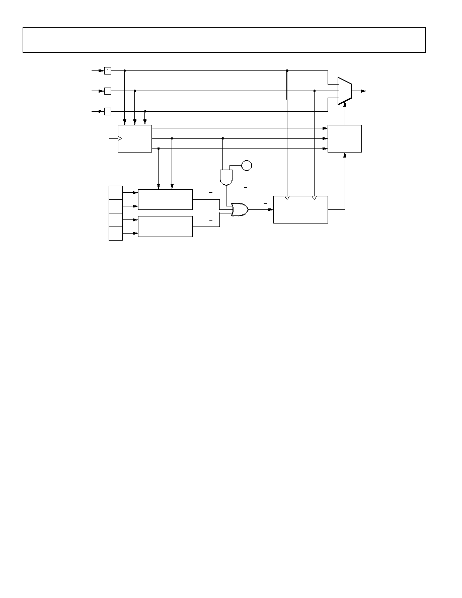
Figure 29. Switchover/Holdover Block Diagram
The user can override the automatic switchover functions
(revertive and nonrevertive) and manually select the REFA
or REFB signal by programming Register 0x29[7:6] = 10 or 11,
respectively. Note, however, that the desired signal (REFA or
REFB) must be present for the device to select it.
The user can also force the device to switch to REFB by applying
a Logic 1 to the external SEL REFB pin. This overrides a REFA
selection invoked by either the revertive/nonrevertive logic or
when Register 0x29[7:6] = 10. Note, however, that REFB must
be present to be selected by the device.
PLL (PFD, Charge Pump, VCO, Feedback Divider)
The PLL (see Figure 27) consists of a phase/frequency detector
(PFD), a partially integrated analog loop filter (see Figure 30),
an integrated voltage controlled oscillator (VCO), and a 20-bit
programmable feedback divider. The PLL generates a 3.35 GHz
to 4.05 GHz clock signal that is phase locked to the active input
reference signal, and its frequency is the phase detector frequency
(FPFD) multiplied by the feedback divider value (N).
The PFD of the PLL drives a charge pump that increases, decreases,
or holds constant the charge stored on the loop filter capacitors
(both internal and external). The stored charge results in a voltage
that sets the output frequency of the VCO. The feedback loop of
the PLL causes the VCO control voltage to vary in such a way as
to phase lock the PFD input signals. Note that the PFD supports
input frequencies spanning 13.3 kHz to 100 MHz (implying that
input frequencies between 8 kHz and 13.3 kHz must use the ×2
frequency multiplier in the input path).
The PLL has a VCO with 128 frequency bands spanning a range
of 3350 MHz to 4050 MHz (3700 MHz nominal). However, the
actual operating frequency within a particular band depends on
the control voltage that appears on the loop filter capacitor. The
control voltage causes the VCO output frequency to vary linearly
within the selected band. This frequency variability allows the
control loop of the PLL to synchronize the VCO output signal
with the reference signal applied to the PFD.
Typically, selection of the VCO frequency band (as well as gain
adjustment) occurs automatically as part of the automatic VCO
calibration process of the device, which initiates at power up (or
reset). Alternatively, the user can force VCO calibration by first
enabling SPI control of VCO calibration (Register 0x0E[2] = 1)
and then writing a 1 to the calibrate VCO bit (Register 0x0E[7]).
Note that VCO calibration centers the dc operating point of the
VCO control signal. Furthermore, during VCO calibration, the
output drivers provide a static dc signal.
To facilitate system debugging, the user can override the VCO band
setting by first enabling SPI control of VCO band (Register 0x0E[0]
= 1) and then writing the desired value to Register 0x10[7:1].
The feedback divider (N-divider) sets the frequency multi-
plication factor of the PLL in integer steps over a 20-bit range.
Note that the N-divider has a lower limit of 32.
相关PDF资料 |
PDF描述 |
|---|---|
| MS27467T25F2P | CONN PLUG 100POS STRAIGHT W/PINS |
| AD9550BCPZ | IC INTEGER-N TRANSLATOR 32-LFCSP |
| AD9573ARUZ | IC PCI CLCOK GEN 25MHZ 16TSSOP |
| MS3452W24-22PW | CONN RCPT 4POS BOX MNT W/PINS |
| MS3452W24-22P | CONN RCPT 4POS BOX MNT W/PINS |
相关代理商/技术参数 |
参数描述 |
|---|---|
| AD9553BCPZ-REEL7 | 功能描述:IC INTEGER-N CLCK GEN 32LFCSP RoHS:是 类别:集成电路 (IC) >> 时钟/计时 - 专用 系列:- 标准包装:28 系列:- 类型:时钟/频率发生器 PLL:是 主要目的:Intel CPU 服务器 输入:时钟 输出:LVCMOS 电路数:1 比率 - 输入:输出:3:22 差分 - 输入:输出:无/是 频率 - 最大:400MHz 电源电压:3.135 V ~ 3.465 V 工作温度:0°C ~ 85°C 安装类型:表面贴装 封装/外壳:64-TFSOP (0.240",6.10mm 宽) 供应商设备封装:64-TSSOP 包装:管件 |
| AD9554/PCBZ | 功能描述:AD9554 - Timing, Clock Generator Evaluation Board 制造商:analog devices inc. 系列:- 零件状态:有效 主要用途:计时,时钟发生器 嵌入式:- 使用的 IC/零件:AD9554 主要属性:- 辅助属性:LED 状态指示器 所含物品:板 标准包装:1 |
| AD9554-1/PCBZ | 功能描述:AD9554-1 - Timing, Clock Generator Evaluation Board 制造商:analog devices inc. 系列:- 零件状态:有效 主要用途:计时,时钟发生器 嵌入式:- 使用的 IC/零件:AD9554-1 主要属性:- 辅助属性:LED 状态指示器 所含物品:板 标准包装:1 |
| AD9554-1BCPZ | 功能描述:IC PLL CLOCK GEN 4OUT 72LFCSP 制造商:analog devices inc. 系列:- 包装:托盘 零件状态:有效 PLL:是 主要用途:以太网,SONET/SDH,Stratum 输入:CMOS,LVDS 输出:HCSL,LVDS,LVPECL 电路数:1 比率 - 输入:输出:4:4 差分 - 输入:输出:是/是 频率 - 最大值:942MHz 电压 - 电源:1.4 V ~ 2.625 V 工作温度:-40°C ~ 85°C 安装类型:表面贴装 封装/外壳:56-WFQFN 裸焊盘,CSP 供应商器件封装:56-LFCSP-WQ(8x8) 标准包装:1 |
| AD9554-1BCPZ-REEL7 | 功能描述:IC PLL CLOCK GEN 4OUT 72LFCSP 制造商:analog devices inc. 系列:- 包装:带卷(TR) 零件状态:有效 PLL:是 主要用途:以太网,SONET/SDH,Stratum 输入:CMOS,LVDS 输出:HCSL,LVDS,LVPECL 电路数:1 比率 - 输入:输出:4:4 差分 - 输入:输出:是/是 频率 - 最大值:942MHz 电压 - 电源:1.4 V ~ 2.625 V 工作温度:-40°C ~ 85°C 安装类型:表面贴装 封装/外壳:56-WFQFN 裸焊盘,CSP 供应商器件封装:56-LFCSP-WQ(8x8) 标准包装:750 |
发布紧急采购,3分钟左右您将得到回复。