- 您现在的位置:买卖IC网 > PDF目录17025 > AD9609-20EBZ (Analog Devices Inc)BOARD EVALUATION AD9609 20MSPS PDF资料下载
参数资料
| 型号: | AD9609-20EBZ |
| 厂商: | Analog Devices Inc |
| 文件页数: | 13/32页 |
| 文件大小: | 0K |
| 描述: | BOARD EVALUATION AD9609 20MSPS |
| 设计资源: | AD9649/29/09 Schematics AD9649/29/09 Gerber Files |
| 标准包装: | 1 |
| ADC 的数量: | 1 |
| 位数: | 10 |
| 采样率(每秒): | 20M |
| 数据接口: | 串行,SPI? |
| 输入范围: | 2 Vpp |
| 在以下条件下的电源(标准): | 46.3mW @ 20MSPS |
| 工作温度: | -40°C ~ 85°C |
| 已用 IC / 零件: | AD9609 |
| 已供物品: | 板 |
第1页第2页第3页第4页第5页第6页第7页第8页第9页第10页第11页第12页当前第13页第14页第15页第16页第17页第18页第19页第20页第21页第22页第23页第24页第25页第26页第27页第28页第29页第30页第31页第32页
AD9609
Rev. 0 | Page 20 of 32
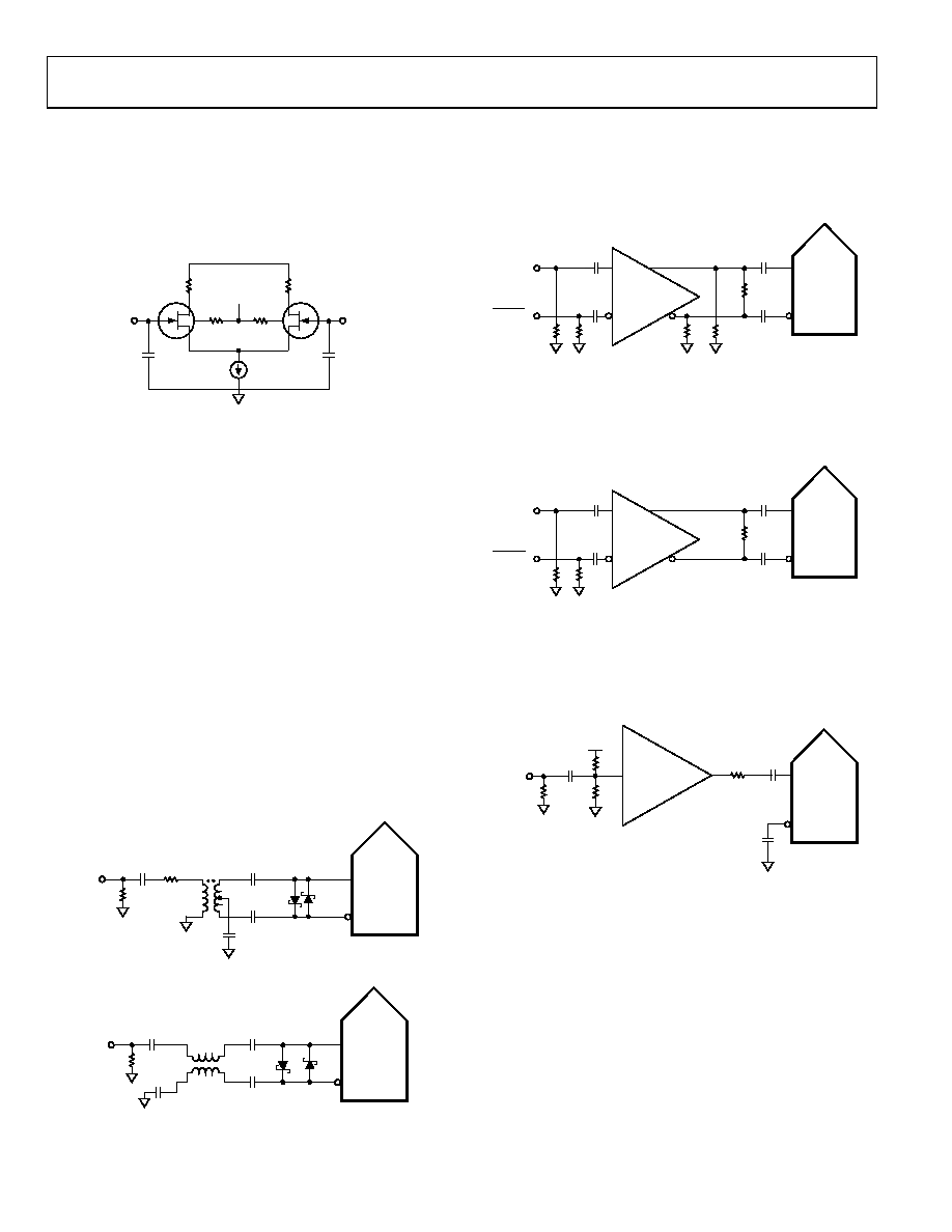
CLOCK INPUT CONSIDERATIONS
For optimum performance, clock the AD9609 sample clock
inputs, CLK+ and CLK, with a differential signal. The signal
is typically ac-coupled into the CLK+ and CLK pins via a
transformer or capacitors. These pins are biased internally
(see Figure 45) and require no external bias.
0.9V
AVDD
2pF
CLK–
CLK+
08
54
1-
0
16
Figure 45. Equivalent Clock Input Circuit
Clock Input Options
The AD9609 has a very flexible clock input structure. The clock
input can be a CMOS, LVDS, LVPECL, or sine wave signal.
Regardless of the type of signal being used, clock source jitter is
of great concern, as described in the Jitter Considerations section.
ing the AD9609 (at clock rates up to 625 MHz). A low jitter clock
source is converted from a single-ended signal to a differential
signal using either an RF transformer or an RF balun.
The RF balun configuration is recommended for clock frequencies
between 125 MHz and 625 MHz, and the RF transformer is
recommended for clock frequencies from 10 MHz to 200 MHz.
The back-to-back Schottky diodes across the transformer/
balun secondary limit clock excursions into the AD9609 to
approximately 0.8 V p-p differential.
This limit helps prevent the large voltage swings of the clock
from feeding through to other portions of the AD9609 while
preserving the fast rise and fall times of the signal that are
critical to a low jitter performance.
0.1F
SCHOTTKY
DIODES:
HSMS2822
CLOCK
INPUT
50
100
CLK–
CLK+
ADC
Mini-Circuits
ADT1-1WT, 1:1 Z
XFMR
08
54
1-
0
17
Figure 46. Transformer-Coupled Differential Clock (Up to 200 MHz)
0.1F
1nF
CLOCK
INPUT
1nF
50
CLK–
CLK+
SCHOTTKY
DIODES:
HSMS2822
ADC
08
54
1-
01
8
Figure 47. Balun-Coupled Differential Clock (Up to 625 MHz)
If a low jitter clock source is not available, another option is to
ac couple a differential PECL signal to the sample clock input
excellent jitter performance.
100
0.1F
240
240
50k
50k
CLK–
CLK+
CLOCK
INPUT
CLOCK
INPUT
ADC
AD951x
PECL DRIVER
0
854
1-
01
9
Figure 48. Differential PECL Sample Clock (Up to 625 MHz)
A third option is to ac couple a differential LVDS signal to the
clock drivers offer excellent jitter performance.
100
0.1F
50k
50k
CLK–
CLK+
ADC
CLOCK
INPUT
CLOCK
INPUT
AD951x
LVDS DRIVER
0
854
1-
020
Figure 49. Differential LVDS Sample Clock (Up to 625 MHz)
In some applications, it may be acceptable to drive the sample
clock inputs with a single-ended 1.8 V CMOS signal. In such
applications, drive the CLK+ pin directly from a CMOS gate, and
bypass the CLK pin to ground with a 0.1 μF capacitor (see
OPTIONAL
100
0.1F
50
1
150
RESISTOR IS OPTIONAL.
CLK–
CLK+
ADC
VCC
1k
1k
CLOCK
INPUT
AD951x
CMOS DRIVER
08
54
1-
02
1
Figure 50. Single-Ended 1.8 V CMOS Input Clock (Up to 200 MHz)
Input Clock Divider
The AD9609 contains an input clock divider with the ability
to divide the input clock by integer values between 1 and 8.
Optimum performance can be obtained by enabling the inter-
nal duty cycle stabilizer (DCS) when using divide ratios other
than 1, 2, or 4.
相关PDF资料 |
PDF描述 |
|---|---|
| 0210490970 | CABLE JUMPER 1.25MM .102M 27POS |
| 0210490242 | CABLE JUMPER 1.25MM .127M 18POS |
| EBM30DRSH | CONN EDGECARD 60POS DIP .156 SLD |
| RBM18DRMH | CONN EDGECARD 36POS .156 WW |
| AD9609-65EBZ | BOARD EVALUATION AD9609 65MSPS |
相关代理商/技术参数 |
参数描述 |
|---|---|
| AD9609-40EBZ | 功能描述:BOARD EVALUATION AD9609 40MSPS RoHS:是 类别:编程器,开发系统 >> 评估板 - 模数转换器 (ADC) 系列:- 产品培训模块:Obsolescence Mitigation Program 标准包装:1 系列:- ADC 的数量:1 位数:12 采样率(每秒):94.4k 数据接口:USB 输入范围:±VREF/2 在以下条件下的电源(标准):- 工作温度:-40°C ~ 85°C 已用 IC / 零件:MAX11645 已供物品:板,软件 |
| AD9609-65EBZ | 功能描述:BOARD EVALUATION AD9609 65MSPS RoHS:是 类别:编程器,开发系统 >> 评估板 - 模数转换器 (ADC) 系列:- 产品培训模块:Obsolescence Mitigation Program 标准包装:1 系列:- ADC 的数量:1 位数:12 采样率(每秒):94.4k 数据接口:USB 输入范围:±VREF/2 在以下条件下的电源(标准):- 工作温度:-40°C ~ 85°C 已用 IC / 零件:MAX11645 已供物品:板,软件 |
| AD9609-80EBZ | 功能描述:BOARD EVALUATION AD9609 80MSPS RoHS:是 类别:编程器,开发系统 >> 评估板 - 模数转换器 (ADC) 系列:- 产品培训模块:Obsolescence Mitigation Program 标准包装:1 系列:- ADC 的数量:1 位数:12 采样率(每秒):94.4k 数据接口:USB 输入范围:±VREF/2 在以下条件下的电源(标准):- 工作温度:-40°C ~ 85°C 已用 IC / 零件:MAX11645 已供物品:板,软件 |
| AD9609BCPZ-20 | 功能描述:IC ADC 10BIT 20MSPS LP 32LFCSP RoHS:是 类别:集成电路 (IC) >> 数据采集 - 模数转换器 系列:- 标准包装:1 系列:microPOWER™ 位数:8 采样率(每秒):1M 数据接口:串行,SPI? 转换器数目:1 功率耗散(最大):- 电压电源:模拟和数字 工作温度:-40°C ~ 125°C 安装类型:表面贴装 封装/外壳:24-VFQFN 裸露焊盘 供应商设备封装:24-VQFN 裸露焊盘(4x4) 包装:Digi-Reel® 输入数目和类型:8 个单端,单极 产品目录页面:892 (CN2011-ZH PDF) 其它名称:296-25851-6 |
| AD9609BCPZ-40 | 功能描述:IC ADC 10BIT 40MSPS LP 32LFCSP RoHS:是 类别:集成电路 (IC) >> 数据采集 - 模数转换器 系列:- 标准包装:1 系列:microPOWER™ 位数:8 采样率(每秒):1M 数据接口:串行,SPI? 转换器数目:1 功率耗散(最大):- 电压电源:模拟和数字 工作温度:-40°C ~ 125°C 安装类型:表面贴装 封装/外壳:24-VFQFN 裸露焊盘 供应商设备封装:24-VQFN 裸露焊盘(4x4) 包装:Digi-Reel® 输入数目和类型:8 个单端,单极 产品目录页面:892 (CN2011-ZH PDF) 其它名称:296-25851-6 |
发布紧急采购,3分钟左右您将得到回复。