- 您现在的位置:买卖IC网 > PDF目录10199 > AD9629BCPZRL7-65 (Analog Devices Inc)IC ADC 12BIT 65MSPS 32LFCSP PDF资料下载
参数资料
| 型号: | AD9629BCPZRL7-65 |
| 厂商: | Analog Devices Inc |
| 文件页数: | 2/32页 |
| 文件大小: | 0K |
| 描述: | IC ADC 12BIT 65MSPS 32LFCSP |
| 标准包装: | 1,500 |
| 位数: | 12 |
| 采样率(每秒): | 65M |
| 数据接口: | 串行,SPI? |
| 转换器数目: | 1 |
| 功率耗散(最大): | 86mW |
| 电压电源: | 模拟和数字 |
| 工作温度: | -40°C ~ 85°C |
| 安装类型: | 表面贴装 |
| 封装/外壳: | 32-VFQFN 裸露焊盘,CSP |
| 供应商设备封装: | 32-LFCSP-VQ |
| 包装: | 带卷 (TR) |
| 输入数目和类型: | 2 个单端,单极;1 个差分,单极 |
第1页当前第2页第3页第4页第5页第6页第7页第8页第9页第10页第11页第12页第13页第14页第15页第16页第17页第18页第19页第20页第21页第22页第23页第24页第25页第26页第27页第28页第29页第30页第31页第32页
AD9629
Rev. 0 | Page 10 of 32
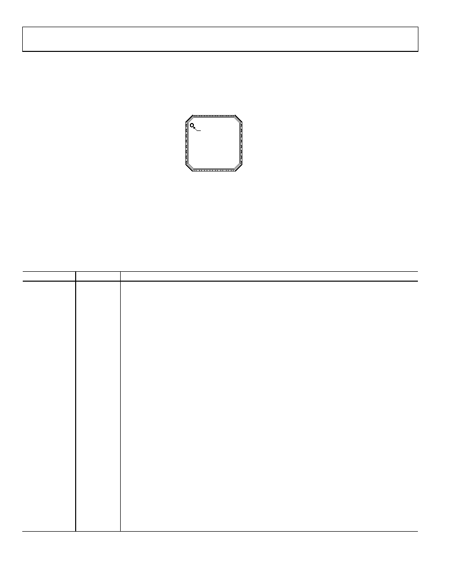
PIN CONFIGURATION AND FUNCTION DESCRIPTIONS
PIN 1
INDICATOR
1
CLK+
2
CLK–
3
AVDD
4
CSB
5
SCLK/DFS
6
SDIO/PDWN
7
NC
8
NC
24 AVDD
23 MODE/OR
22 DCO
21 D11 (MSB)
20 D10
19 D9
18 D8
17 D7
9
(L
S
B
)
D
0
1
0
D
1
D
2
1
2
D
3
1
3
D
R
V
D
1
4
D
4
1
5
D
5
1
6
D
6
3
2
A
V
D
3
1
V
IN
+
3
0
V
IN
–
2
9
A
V
D
2
8
R
B
IA
S
2
7
V
C
M
2
6
S
E
N
S
E
2
5
V
R
E
F
TOP VIEW
(Not to Scale)
AD9629
08
54
0-
0
03
NOTES
1. NC = NO CONNECT.
2. THE EXPOSED PADDLE MUST BE SOLDERED TO
THE PCB GROUND TO ENSURE PROPER HEAT DISSIPATION,
NOISE, AND MECHANICAL STRENGTH BENEFITS.
Figure 3. Pin Configuration
Table 8. Pin Function Description
Pin No.
Mnemonic
Description
0 (EPAD)
GND
Exposed Paddle. The exposed paddle is the only ground connection. It must be soldered to the analog
ground of the customer’s PCB to ensure proper functionality and maximize heat dissipation, noise, and
mechanical strength benefits.
1, 2
CLK+, CLK
Differential Encode Clock. PECL, LVDS, or 1.8 V CMOS inputs.
3, 24, 29, 32
AVDD
1.8 V Supply Pin for ADC Core Domain.
4
CSB
SPI Chip Select. Active low enable. 30 kΩ internal pull-up.
5
SCLK/DFS
SPI Clock Input in SPI Mode (SCLK). 30 kΩ internal pull-down.
Data Format Select in Non-SPI Mode (DFS). Static control of data output format. 30 kΩ internal pull-down.
DFS high = twos complement output; DFS low = offset binary output.
6
SDIO/PDWN
SPI Data Input/Output (SDIO). Bidirectional SPI data I/O in SPI mode. 30 kΩ internal pull-down.
Non-SPI Mode Power-Down (PDWN). Static control of power-down with 30 kΩ internal pull-down. See
Table 14 for details.
7, 8
NC
Do Not Connect.
9 to 12, 14 to 21
D0 (LSB) to
D11 (MSB)
ADC Digital Outputs.
13
DRVDD
1.8 V to 3.3 V Supply Pin for Output Driver Domain.
22
DCO
Data Clock Digital Output.
23
MODE/OR
Chip Mode Select Input or Out-of-Range (OR) Digital Output in SPI Mode.
Default = out-of-range (OR) digital output (SPI Register 0x2A[0] = 1).
Option = chip mode select input (SPI Register 0x2A[0] = 0).
Chip power down (SPI Register 0x08[7:5] = 100b).
Chip standby (SPI Register 0x08[7:5] = 101b).
Normal operation, output disabled (SPI Register 0x08[7:5] = 110b).
Normal operation, output enabled (SPI Register 0x08[7:5] = 111b).
Out-of-Range (OR) digital output only in non-SPI mode.
25
VREF
1.0 V Voltage Reference Input/Output. See Table 10.
26
SENSE
Reference Mode Selection. See Table 10.
27
VCM
Analog Output Voltage at Mid AVDD Supply. Sets common mode of the analog inputs.
28
RBIAS
Sets Analog Current Bias. Connect to 10 kΩ (1% tolerance) resistor to ground.
30, 31
VIN, VIN+
ADC Analog Inputs.
相关PDF资料 |
PDF描述 |
|---|---|
| AD7575AQ | IC ADC 8BIT LC2MOS W/HOLD 18CDIP |
| LTC1282BCSW#TRPBF | IC A/D CONV SAMPLING W/REF24SOIC |
| LTC1278-4ISW#TR | IC ADC 12BIT SAMPL SHTDWN 24SOIC |
| MS27656T17B26SA | CONN RCPT 26POS WALL MNT W/SCKT |
| MS27505E17B35S | CONN RCPT 55POS BOX MNT W/SCKT |
相关代理商/技术参数 |
参数描述 |
|---|---|
| AD9629BCPZRL7-80 | 功能描述:IC ADC 12BIT 80MSPS 32LFCSP RoHS:是 类别:集成电路 (IC) >> 数据采集 - 模数转换器 系列:- 标准包装:1 系列:- 位数:14 采样率(每秒):83k 数据接口:串行,并联 转换器数目:1 功率耗散(最大):95mW 电压电源:双 ± 工作温度:0°C ~ 70°C 安装类型:通孔 封装/外壳:28-DIP(0.600",15.24mm) 供应商设备封装:28-PDIP 包装:管件 输入数目和类型:1 个单端,双极 |
| AD9629XCPZ-40 | 功能描述:IC ADC 12BIT 40MSPS 制造商:analog devices inc. 系列:* 零件状态:上次购买时间 标准包装:1 |
| AD9630 | 制造商:AD 制造商全称:Analog Devices 功能描述:Low Distortion 750 MHz Closed-Loop Buffer Amp |
| AD9630AN | 制造商:AD 制造商全称:Analog Devices 功能描述:Low Distortion 750 MHz Closed-Loop Buffer Amp |
发布紧急采购,3分钟左右您将得到回复。