- 您现在的位置:买卖IC网 > PDF目录165343 > AD9643BCPZ-250 (ANALOG DEVICES INC) 2-CH 14-BIT FLASH METHOD ADC, PARALLEL ACCESS, QCC64 PDF资料下载
参数资料
| 型号: | AD9643BCPZ-250 |
| 厂商: | ANALOG DEVICES INC |
| 元件分类: | ADC |
| 英文描述: | 2-CH 14-BIT FLASH METHOD ADC, PARALLEL ACCESS, QCC64 |
| 封装: | 9 X 9 MM, ROHS COMPLIANT, MO-220VMMD-4, LFCSP-64 |
| 文件页数: | 16/36页 |
| 文件大小: | 1659K |
| 代理商: | AD9643BCPZ-250 |
第1页第2页第3页第4页第5页第6页第7页第8页第9页第10页第11页第12页第13页第14页第15页当前第16页第17页第18页第19页第20页第21页第22页第23页第24页第25页第26页第27页第28页第29页第30页第31页第32页第33页第34页第35页第36页
AD9643
Rev. A | Page 23 of 36
THEORY OF OPERATION
The AD9643 has two analog input channels and two digital
output channels. The intermediate frequency (IF) signal passes
through several stages before appearing at the output port(s).
The dual ADC design can be used for diversity reception of signals,
where the ADCs operate identically on the same carrier but from
two separate antennae. The ADCs can also be operated with
independent analog inputs. The user can sample frequencies
from dc to 300 MHz using appropriate low-pass or band-pass
filtering at the ADC inputs with little loss in ADC performance.
Operation to 400 MHz analog input is permitted but occurs at
the expense of increased ADC noise and distortion.
Synchronization capability is provided to allow synchronized
timing between multiple devices.
Programming and control of the AD9643 are accomplished
using a 3-pin, SPI-compatible serial interface.
ADC ARCHITECTURE
The AD9643 architecture consists of a dual front-end sample-
and-hold circuit, followed by a pipelined switched-capacitor
ADC. The quantized outputs from each stage are combined into
a final 14-bit result in the digital correction logic. The pipelined
architecture permits the first stage to operate on a new input
sample and the remaining stages to operate on the preceding
samples. Sampling occurs on the rising edge of the clock.
Each stage of the pipeline, excluding the last, consists of a low
resolution flash ADC connected to a switched-capacitor digital-
to-analog converter (DAC) and an interstage residue amplifier
(MDAC). The MDAC magnifies the difference between the recon-
structed DAC output and the flash input for the next stage in
the pipeline. One bit of redundancy is used in each stage to
facilitate digital correction of flash errors. The last stage simply
consists of a flash ADC.
The input stage of each channel contains a differential sampling
circuit that can be ac- or dc-coupled in differential or single-
ended modes. The output staging block aligns the data, corrects
errors, and passes the data to the output buffers. The output buffers
are powered from a separate supply, allowing digital output noise to
be separated from the analog core. During power-down, the
output buffers go into a high impedance state.
ANALOG INPUT CONSIDERATIONS
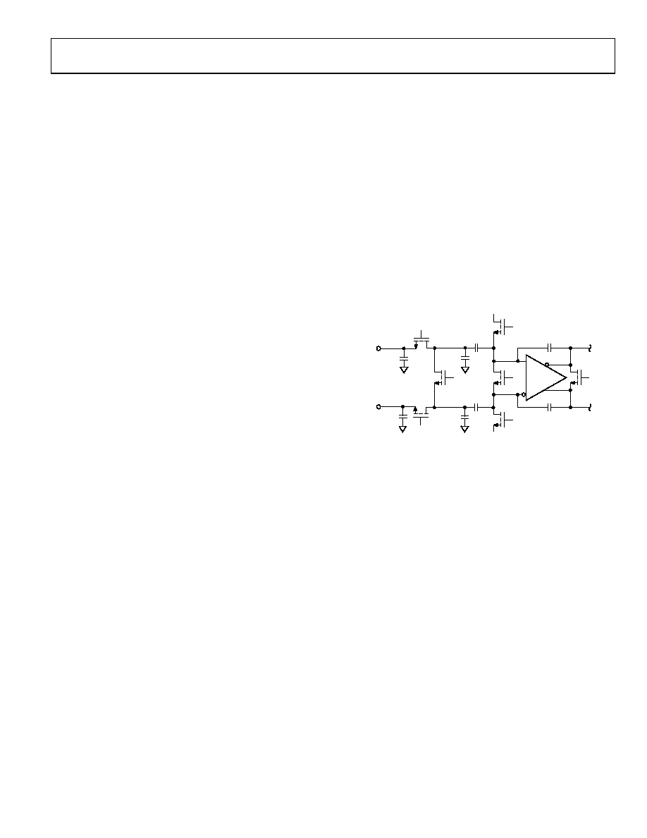
The analog input to the AD9643 is a differential switched-
capacitor circuit that has been designed for optimum performance
while processing a differential input signal.
The clock signal alternatively switches the input between sample
mode and hold mode (see the configuration shown in Figure 46).
When the input is switched into sample mode, the signal source
must be capable of charging the sampling capacitors and settling
within 1/2 clock cycle.
A small resistor in series with each input can help reduce the
peak transient current required from the output stage of the
driving source. A shunt capacitor can be placed across the
inputs to provide dynamic charging currents. This passive
network creates a low-pass filter at the ADC input; therefore,
the precise values are dependent on the application.
In intermediate frequency (IF) undersampling applications, the
shunt capacitors should be reduced. In combination with the
driving source impedance, the shunt capacitors limit the input
bandwidth. Refer to the AN-742 Application Note, Frequency
Domain Response of Switched-Capacitor ADCs; the AN-827
Application Note, A Resonant Approach to Interfacing Amplifiers to
Switched-Capacitor ADCs; and the Analog Dialogue article,
for more information on this subject.
CPAR1
CPAR2
S
CFB
CS
BIAS
VIN+
09
63
6-
0
50
H
VIN–
Figure 46. Switched-Capacitor Input
For best dynamic performance, the source impedances driving
VIN+ and VIN should be matched, and the inputs should be
differentially balanced.
Input Common Mode
The analog inputs of the AD9643 are not internally dc biased.
In ac-coupled applications, the user must provide this bias
externally. Setting the device so that VCM = 0.5 × AVDD (or
0.9 V) is recommended for optimum performance. An on-board
common-mode voltage reference is included in the design and is
available from the VCM pin. Using the VCM output to set the
input common mode is recommended. Optimum performance
is achieved when the common-mode voltage of the analog input
is set by the VCM pin voltage (typically 0.5 × AVDD). The
VCM pin must be decoupled to ground by a 0.1 μF capacitor, as
described in the Applications Information section. This
decoupling capacitor should be placed close to the pin to
minimize the series resistance and inductance between the part
and this capacitor.
Differential Input Configurations
Optimum performance is achieved while driving the AD9643
in a differential input configuration. For baseband applications,
相关PDF资料 |
PDF描述 |
|---|---|
| AD9643BCPZRL7-210 | 2-CH 14-BIT FLASH METHOD ADC, PARALLEL ACCESS, QCC64 |
| AD9753ASTZRL | PARALLEL, WORD INPUT LOADING, 0.011 us SETTLING TIME, 12-BIT DAC, PQFP48 |
| ADA123AL7 | FIBER OPTIC ADD/DROP MUX/DEMUX, LC/UPC CONNECTOR |
| ADA123AB1 | FIBER OPTIC ADD/DROP MUX/DEMUX, FC/PC CONNECTOR |
| ADA123AB2 | FIBER OPTIC ADD/DROP MUX/DEMUX, FC/APC CONNECTOR |
相关代理商/技术参数 |
参数描述 |
|---|---|
| AD9643BCPZRL7-170 | 功能描述:模数转换器 - ADC 14 Bit 170Msps Dual ADC RoHS:否 制造商:Analog Devices 通道数量: 结构: 转换速率: 分辨率: 输入类型: 信噪比: 接口类型: 工作电源电压: 最大工作温度: 安装风格: 封装 / 箱体: |
| AD9643BCPZRL7-210 | 功能描述:模数转换器 - ADC 14 Bit 210Msps Dual ADC RoHS:否 制造商:Analog Devices 通道数量: 结构: 转换速率: 分辨率: 输入类型: 信噪比: 接口类型: 工作电源电压: 最大工作温度: 安装风格: 封装 / 箱体: |
| AD9643BCPZRL7-250 | 功能描述:模数转换器 - ADC 14 Bit 250Msps Dual ADC RoHS:否 制造商:Analog Devices 通道数量: 结构: 转换速率: 分辨率: 输入类型: 信噪比: 接口类型: 工作电源电压: 最大工作温度: 安装风格: 封装 / 箱体: |
| AD9644-155KITZ | 功能描述:KIT EVAL FOR AD9644 RoHS:是 类别:编程器,开发系统 >> 评估板 - 模数转换器 (ADC) 系列:* 产品培训模块:Obsolescence Mitigation Program 标准包装:1 系列:- ADC 的数量:1 位数:12 采样率(每秒):94.4k 数据接口:USB 输入范围:±VREF/2 在以下条件下的电源(标准):- 工作温度:-40°C ~ 85°C 已用 IC / 零件:MAX11645 已供物品:板,软件 |
| AD9644-80KITZ | 功能描述:BOARD EVALUATION FOR AD9644 RoHS:是 类别:编程器,开发系统 >> 评估板 - 模数转换器 (ADC) 系列:- 产品培训模块:Obsolescence Mitigation Program 标准包装:1 系列:- ADC 的数量:1 位数:12 采样率(每秒):94.4k 数据接口:USB 输入范围:±VREF/2 在以下条件下的电源(标准):- 工作温度:-40°C ~ 85°C 已用 IC / 零件:MAX11645 已供物品:板,软件 |
发布紧急采购,3分钟左右您将得到回复。