参数资料
| 型号: | AD9779BSVZ |
| 厂商: | Analog Devices Inc |
| 文件页数: | 39/56页 |
| 文件大小: | 0K |
| 描述: | IC DAC 16BIT DUAL 1GSPS 100TQFP |
| 产品培训模块: | Data Converter Fundamentals DAC Architectures |
| 标准包装: | 1 |
| 位数: | 16 |
| 数据接口: | 串行 |
| 转换器数目: | 2 |
| 电压电源: | 模拟和数字 |
| 功率耗散(最大): | 300mW |
| 工作温度: | -40°C ~ 85°C |
| 安装类型: | 表面贴装 |
| 封装/外壳: | 100-TQFP 裸露焊盘 |
| 供应商设备封装: | 100-TQFP-EP(14x14) |
| 包装: | 托盘 |
| 输出数目和类型: | 4 电流,单极 |
| 采样率(每秒): | 1G |
第1页第2页第3页第4页第5页第6页第7页第8页第9页第10页第11页第12页第13页第14页第15页第16页第17页第18页第19页第20页第21页第22页第23页第24页第25页第26页第27页第28页第29页第30页第31页第32页第33页第34页第35页第36页第37页第38页当前第39页第40页第41页第42页第43页第44页第45页第46页第47页第48页第49页第50页第51页第52页第53页第54页第55页第56页
AD9776/AD9778/AD9779
Rev. A | Page 44 of 56
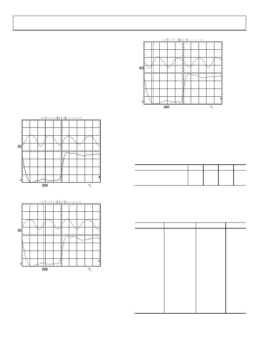
Using Data Delay to Meet Timing Requirements
To meet strict timing requirements at input data rates of up to
250 MSPS, the AD977x has a fine timing feature. Fine timing
adjustments are made by programming values into the data
clock delay register (Register 0x04, Bits<7:4>). This register can
be used to add delay between the REFCLK in and the
DATACLK out. Figure 97 shows the default delay present when
DATACLK delay is disabled. The disable function bit is found
in Register 0x02, Bit 4. Figure 98 shows the delay present when
DATACLK delay is enabled and set to 0000. Figure 99 indicates
the delay when DATACLK delay is enabled and set to 1111.
Note that the setup and hold times specified for data to
DATACLK are defined for DATACLK delay disabled.
CH1 1.00V
Ω
TEK RUN: 5.00GS/s
SAMPLE
CH2 500mV
Ω
M2.00ns
CH1
420mV
Δ: 4.48nS
@: 40.28nS
2
1
05361-089
Figure 97. Delay from REFCLK to DATACLK with DATACLK Delay Disabled
CH1 1.00V
Ω
TEK RUN: 5.00GS/s
SAMPLE
CH2 500mV
Ω
M2.00ns
CH1
420mV
Δ: 4.76nS
@: 35.52nS
2
1
05361-090
Figure 98. Delay from REFCLK to DATACLK Out with DATACLK Delay = 0000
CH1 1.00V
Ω
TEK RUN: 5.00GS/s
SAMPLE
CH2 500mV
Ω
M2.00ns
CH1
420mV
Δ: 7.84nS
@: 32.44nS
2
1
05361-091
Figure 99. Delay from REFCLK to DATACLK Out with DATACLK Delay = 1111
The difference between the minimum delay shown in Figure 98
and the maximum delay shown in Figure 99 is the range
programmable using the DATACLK delay register. The delay
(in absolute time) when programming DATACLK delay
between 0000 and 1111 is a linear extrapolation between these
two figures. The typical delays per increment over temperature
are shown in Table 20.
Table 20. Data Delay Line Typical Delays Over Temperature
Delays
40°C
+25°C
+85°C
Unit
Delay Between Disabled and
Enabled
370
416
432
ps
Average Delay per Increment
171
183
197
ps
The frequency of DATACLK out depends on several program-
mable settings: interpolation, zero stuffing, and interleaved/
dual port mode, all of which have an effect on the REFCLK
frequency. The divisor function between REFCLK and
DATACLK is equal to the values shown in Table 21.
Table 21. REFCLK to DATACLK Divisor Ratio
Interpolation
Zero Stuffing
Input Mode
Divisor
1
Disabled
Dual port
1
2
Disabled
Dual port
2
4
Disabled
Dual port
4
8
Disabled
Dual port
8
1
Disabled
Interleaved
Invalid
2
Disabled
Interleaved
1
4
Disabled
Interleaved
2
8
Disabled
Interleaved
4
1
Enabled
Dual port
2
Enabled
Dual port
4
Enabled
Dual port
8
Enabled
Dual port
16
1
Enabled
Interleaved
1
2
Enabled
Interleaved
2
4
Enabled
Interleaved
4
8
Enabled
Interleaved
8
相关PDF资料 |
PDF描述 |
|---|---|
| AD9786BSVZRL | IC DAC 16BIT INTERPOL/SP 80TQFP |
| AD9788BSVZRL | IC DAC 16BIT 800MSPS 100TQFP |
| AD9806KSTZ | IC CCD SIGNAL PROC 10BIT 48LQFP |
| AD9814JR | IC CCD SIGNAL PROC 14BIT 28-SOIC |
| AD9823KRUZRL7 | IC CDS FOR DGTL CAMERA 14-TSSOP |
相关代理商/技术参数 |
参数描述 |
|---|---|
| AD9779BSVZ1 | 制造商:AD 制造商全称:Analog Devices 功能描述:Dual 12-/14-/16-Bit, 1 GSPS, Digital-to-Analog Converters |
| AD9779BSVZRL | 功能描述:IC DAC 16BIT DUAL 1GSPS 100TQFP RoHS:是 类别:集成电路 (IC) >> 数据采集 - 数模转换器 系列:- 产品培训模块:Lead (SnPb) Finish for COTS Obsolescence Mitigation Program 标准包装:1,000 系列:- 设置时间:1µs 位数:8 数据接口:串行 转换器数目:8 电压电源:双 ± 功率耗散(最大):941mW 工作温度:0°C ~ 70°C 安装类型:表面贴装 封装/外壳:24-SOIC(0.295",7.50mm 宽) 供应商设备封装:24-SOIC W 包装:带卷 (TR) 输出数目和类型:8 电压,单极 采样率(每秒):* |
| AD9779BSVZRL1 | 制造商:AD 制造商全称:Analog Devices 功能描述:Dual 12-/14-/16-Bit, 1 GSPS, Digital-to-Analog Converters |
| AD9779-EB | 制造商:Analog Devices 功能描述:EVAL BOARD 16 BIT DUAL INTERPOLATION DAC - Bulk |
| AD9779-EBZ | 制造商:Analog Devices 功能描述:DUAL 16B, 1.0 GSPS TXDAC - Bulk |
发布紧急采购,3分钟左右您将得到回复。