参数资料
| 型号: | AD9785BSVZ |
| 厂商: | Analog Devices Inc |
| 文件页数: | 42/64页 |
| 文件大小: | 0K |
| 描述: | IC DAC 12BIT 800MSPS 100TQFP |
| 产品培训模块: | Data Converter Fundamentals DAC Architectures |
| 标准包装: | 1 |
| 系列: | TxDAC® |
| 位数: | 12 |
| 数据接口: | 串行 |
| 转换器数目: | 2 |
| 电压电源: | 模拟和数字 |
| 功率耗散(最大): | 450mW |
| 工作温度: | -40°C ~ 85°C |
| 安装类型: | 表面贴装 |
| 封装/外壳: | 100-TQFP 裸露焊盘 |
| 供应商设备封装: | 100-TQFP-EP(14x14) |
| 包装: | 托盘 |
| 输出数目和类型: | 2 电流,单极;2 电流,双极 |
| 采样率(每秒): | 800M |
| 产品目录页面: | 785 (CN2011-ZH PDF) |
第1页第2页第3页第4页第5页第6页第7页第8页第9页第10页第11页第12页第13页第14页第15页第16页第17页第18页第19页第20页第21页第22页第23页第24页第25页第26页第27页第28页第29页第30页第31页第32页第33页第34页第35页第36页第37页第38页第39页第40页第41页当前第42页第43页第44页第45页第46页第47页第48页第49页第50页第51页第52页第53页第54页第55页第56页第57页第58页第59页第60页第61页第62页第63页第64页
AD9785/AD9787/AD9788
Rev. A | Page 47 of 64
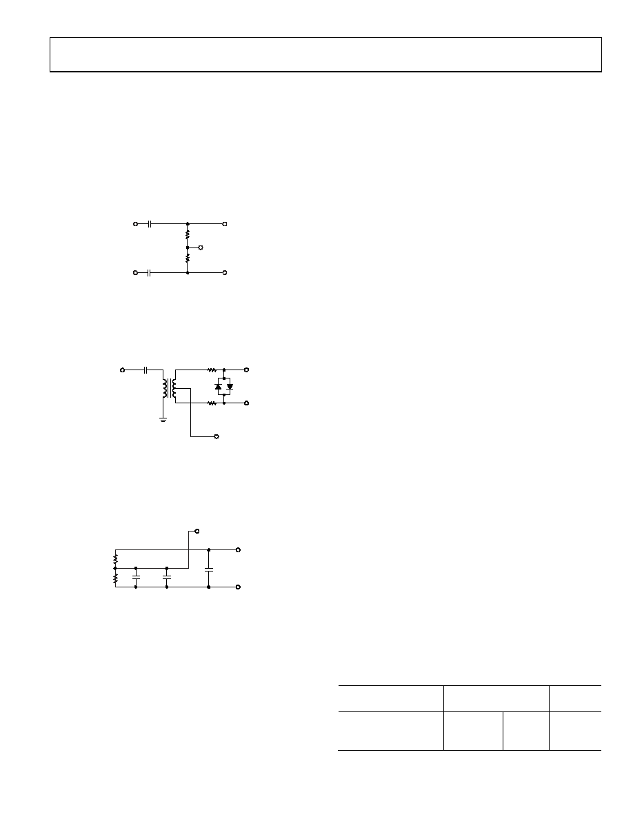
DRIVING THE REFCLK INPUT
The REFCLK input requires a low jitter differential drive signal.
REFCLK is a PMOS input differential pair powered from the 1.8 V
supply; therefore, it is important to maintain the specified 400 mV
input common-mode voltage. Each input pin can safely swing
from 200 mV p-p to 1 V p-p about the 400 mV common-mode
voltage. Although these input levels are not directly LVDS-
compatible, REFCLK can be driven by an offset ac-coupled
LVDS signal, as shown in Figure 65.
LVDS_P_IN
REFCLK+
50
0.1F
LVDS_N_IN
REFCLK–
VCM = 400mV
07
09
8-
02
4
Figure 65. LVDS REFCLK Drive Circuit
If a clean sine clock is available, it can be transformer-coupled
to REFCLK, as shown in Figure 66. Use of a CMOS or TTL
clock is also acceptable for lower sample rates. It can be routed
through a CMOS-to-LVDS translator, then ac-coupled.
50
TTL OR CMOS
CLK INPUT
REFCLK+
REFCLK–
VCM = 400mV
BAV99ZXCT
HIGH SPEED
DUAL DIODE
0.1F
07
09
8-
0
25
Figure 66. TTL or CMOS REFCLK Drive Circuit
It is important to use CVDD18 and CGND for the clock bias
circuit. Any noise or other signal that is coupled onto the clock
is multiplied by the DAC digital input signal and can degrade
DAC performance.
0.1
F1nF
1nF
VCM = 400mV
CVDD18
CGND
1k
287
07
09
8-
0
26
Figure 67. REFCLK VCM Generator Circuit
DAC REFCLK CONFIGURATION
The AD9785/AD9787/AD9788 offer two modes of sourcing
the DAC sample clock (DACCLK). The first mode employs an
on-chip clock multiplier that accepts a reference clock operating
at the lower input frequency, most commonly the data input
frequency. The on-chip phase-locked loop (PLL) then multiplies
the reference clock up to a higher frequency, which can then be
used to generate all the internal clocks required by the DAC.
The clock multiplier provides a high quality clock that meets
the performance requirements of most applications. Using the
on-chip clock multiplier removes the burden of generating and
distributing the high speed DACCLK.
The second mode bypasses the clock multiplier circuitry and
allows DACCLK to be directly sourced through the REFCLK
pins. This mode enables the user to source a very high quality
clock directly to the DAC core. Sourcing the DACCLK directly
through the REFCLK pins may be necessary in demanding
applications that require the lowest possible DAC output noise
at higher output frequencies.
In either case, using the on-chip clock multiplier or sourcing
the DACCLK directly through the REFCLK pins, it is necessary
that the REFCLK signal have low jitter to maximize the DAC
noise performance.
Direct Clocking
When the PLL is disabled (Register 0x04, Bit 15 = 0), the
REFCLK input is used directly as the DAC sample clock
(DACCLK). The output frequency of the DATACLK output
pin is
fDATACLK = fDACCLK/(IF × P)
where IF is the interpolation factor, set in Register 0x01, Bits [7:6],
and P = 0.5 if in single-port mode.
Clock Multiplication
When the PLL is enabled (Register 0x04, Bit 15 = 1), the clock
multiplication circuit generates the DAC sample clock from the
lower rate REFCLK input. The functional diagram of the clock
multiplier is shown in Figure 68.
The clock multiplication circuit operates such that the VCO
outputs a frequency, fVCO, equal to the REFCLK input signal
frequency multiplied by N1 × N2.
fVCO = fREFCLK × (N1 × N2)
The DAC sample clock frequency, fDACCLK, is equal to
fDACCLK = fREFCLK × N2
The values of N1 and N2 must be chosen to keep fVCO in the
optimal operating range of 1.0 GHz to 2.0 GHz. When the VCO
output frequency is known, the correct PLL band select value
(Register 0x04, Bits [7:2]) can be chosen.
PLL Bias Settings
There are three bias settings for the PLL circuitry that should be
programmed to their nominal values. The PLL values shown in
Table 34 are the recommended settings for these parameters.
Table 34. PLL Settings
PLL SPI Control
Address
Optimal
Setting
Register
Bit
PLL Loop Bandwidth
0x04
[20:16]
01111
PLL VCO Drive
0x04
[1:0]
11
PLL Bias
0x04
[10:8]
011
相关PDF资料 |
PDF描述 |
|---|---|
| MS27473E12F3PLC | CONN HSG PLUG 3POS STRGHT PINS |
| VE-J4Z-MZ-S | CONVERTER MOD DC/DC 2V 10W |
| MS27474E24A1S | CONN RCPT 128POS JAM NUT W/SCKT |
| MS27484T10B35B | CONN HSG PLUG 13POS STRGHT SCKT |
| VE-J4Y-MZ-S | CONVERTER MOD DC/DC 3.3V 16.5W |
相关代理商/技术参数 |
参数描述 |
|---|---|
| AD9785BSVZRL | 功能描述:IC DAC 12BIT 800MSPS 100TQFP RoHS:是 类别:集成电路 (IC) >> 数据采集 - 数模转换器 系列:TxDAC® 产品培训模块:Data Converter Fundamentals DAC Architectures 标准包装:750 系列:- 设置时间:7µs 位数:16 数据接口:并联 转换器数目:1 电压电源:双 ± 功率耗散(最大):100mW 工作温度:0°C ~ 70°C 安装类型:表面贴装 封装/外壳:28-LCC(J 形引线) 供应商设备封装:28-PLCC(11.51x11.51) 包装:带卷 (TR) 输出数目和类型:1 电压,单极;1 电压,双极 采样率(每秒):143k |
| AD9785-DPG2-EBZ | 功能描述:BOARD EVALUATION FOR AD9785 RoHS:是 类别:编程器,开发系统 >> 评估板 - 数模转换器 (DAC) 系列:TxDAC® 产品培训模块:Lead (SnPb) Finish for COTS Obsolescence Mitigation Program 标准包装:1 系列:- DAC 的数量:4 位数:12 采样率(每秒):- 数据接口:串行,SPI? 设置时间:3µs DAC 型:电流/电压 工作温度:-40°C ~ 85°C 已供物品:板 已用 IC / 零件:MAX5581 |
| AD9785-EBZ | 制造商:Analog Devices 功能描述:Evaluation Board For AD9785 制造商:Analog Devices 功能描述:DUAL 12B, 1GSPS D-A CONVERTER - Bulk 制造商:Analog Devices 功能描述:Digital to Analog Eval. Board |
| AD9786 | 制造商:AD 制造商全称:Analog Devices 功能描述:16-Bit, 200 MSPS/500 MSPS TxDAC+ with 2】/4】/8】 Interpolation and Signal Processing |
| AD9786BSV | 制造商:Analog Devices 功能描述:DAC 1-CH Interpolation Filter 16-bit 80-Pin TQFP EP 制造商:Analog Devices 功能描述:IC 16BIT DAC SMD 9786 TQFP80 |
发布紧急采购,3分钟左右您将得到回复。