参数资料
| 型号: | AD9785BSVZRL |
| 厂商: | Analog Devices Inc |
| 文件页数: | 15/64页 |
| 文件大小: | 0K |
| 描述: | IC DAC 12BIT 800MSPS 100TQFP |
| 产品培训模块: | Data Converter Fundamentals DAC Architectures |
| 标准包装: | 1,000 |
| 系列: | TxDAC® |
| 位数: | 12 |
| 数据接口: | 串行 |
| 转换器数目: | 2 |
| 电压电源: | 模拟和数字 |
| 功率耗散(最大): | 450mW |
| 工作温度: | -40°C ~ 85°C |
| 安装类型: | 表面贴装 |
| 封装/外壳: | 100-TQFP 裸露焊盘 |
| 供应商设备封装: | 100-TQFP-EP(14x14) |
| 包装: | 带卷 (TR) |
| 输出数目和类型: | 2 电流,单极;2 电流,双极 |
| 采样率(每秒): | 800M |
第1页第2页第3页第4页第5页第6页第7页第8页第9页第10页第11页第12页第13页第14页当前第15页第16页第17页第18页第19页第20页第21页第22页第23页第24页第25页第26页第27页第28页第29页第30页第31页第32页第33页第34页第35页第36页第37页第38页第39页第40页第41页第42页第43页第44页第45页第46页第47页第48页第49页第50页第51页第52页第53页第54页第55页第56页第57页第58页第59页第60页第61页第62页第63页第64页
AD9785/AD9787/AD9788
Rev. A | Page 22 of 64
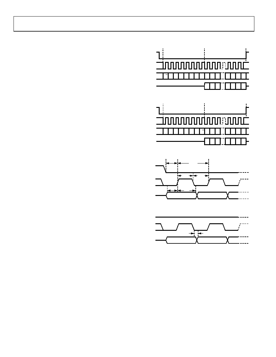
There are two phases to a communication cycle with the
AD9785/AD9787/AD9788. Phase 1 is the instruction cycle,
which is the writing of an instruction byte into the AD9785/
AD9787/AD9788, coincident with the first eight SCLK rising
edges. The instruction byte provides the AD9785/AD9787/
AD9788 serial port controller with information regarding the
data transfer cycle, which is Phase 2 of the communication
cycle. The instruction byte defines whether the upcoming data
transfer is read or write and the serial address of the register
being accessed.
The first eight SCLK rising edges of each communication cycle
are used to write the instruction byte into the AD9785/AD9787/
AD9788. The remaining SCLK edges are for Phase 2 of the
communication cycle. Phase 2 is the actual data transfer
between the AD9785/AD9787/AD9788 and the system
controller. The number of bytes transferred during Phase 2 of
the communication cycle is a function of the register being
accessed.
For example, when accessing the frequency tuning word (FTW)
register, which is four bytes wide, Phase 2 requires that four
bytes be transferred. If accessing the amplitude scale factor (ASF)
register, which is three bytes wide, Phase 2 requires that three
bytes be transferred. After transferring all data bytes per the
instruction byte, the communication cycle is completed.
At the completion of any communication cycle, the AD9785/
AD9787/AD9788 serial port controller expects the next eight
rising SCLK edges to be the instruction byte of the next
communication cycle.
All data input is registered on the rising edge of SCLK. All data
is driven out of the AD9785/AD9787/AD9788 on the falling
edge of SCLK.
Figure 43 through Figure 46 are useful in understanding the
general operation of the AD9785/AD9787/AD9788 serial port.
R/W N1 N0
A4 A3
A2 A1 A0 D7 D6N D5N
D00
D10
D20
D30
D7 D6N D5N
D00
D10
D20
D30
INSTRUCTION CYCLE
DATA TRANSFER CYCLE
SPI_CSB
SCLK
SPI_SDIO
SPI_SDO
07
09
8-
0
06
Figure 43. Serial Register Interface Timing, MSB First
A0 A1 A2
A3 A4
N0 N1 R/W D00 D10 D20
D7N
D6N
D5N
D4N
D00 D10 D20
D7N
D6N
D5N
D4N
INSTRUCTION CYCLE
DATA TRANSFER CYCLE
SPI_CSB
SCLK
SPI_SDIO
SPI_SDO
07
09
8-
0
07
Figure 44. Serial Register Interface Timing, LSB First
INSTRUCTION BIT 6
INSTRUCTION BIT 7
SPI_CSB
SCLK
SPI_SDIO
tDS
tDH
tPWH
tPWL
tSCLK
07
09
8-
00
8
Figure 45. SPI Register Write Timing
DATA BIT n–1
DATA BIT n
SPI_CSB
SCLK
SPI_SDIO
SPI_SDO
tDV
07
09
8-
00
9
Figure 46. SPI Register Read Timing Instruction Byte
相关PDF资料 |
PDF描述 |
|---|---|
| HFA1135IBZ | IC OPAMP CFA 360MHZ LP 8-SOIC |
| LTC2754BIUKG-16#TRPBF | IC DAC 16BIT QUAD IOUT 52-QFN |
| HA3-5020-5Z | IC AMP VIDEO CFA 100MHZ 8-DIP |
| HFA1105IBZ | IC OPAMP CFA 330MHZ LP 8-SOIC |
| VI-B1N-MU | CONVERTER MOD DC/DC 18.5V 200W |
相关代理商/技术参数 |
参数描述 |
|---|---|
| AD9785-DPG2-EBZ | 功能描述:BOARD EVALUATION FOR AD9785 RoHS:是 类别:编程器,开发系统 >> 评估板 - 数模转换器 (DAC) 系列:TxDAC® 产品培训模块:Lead (SnPb) Finish for COTS Obsolescence Mitigation Program 标准包装:1 系列:- DAC 的数量:4 位数:12 采样率(每秒):- 数据接口:串行,SPI? 设置时间:3µs DAC 型:电流/电压 工作温度:-40°C ~ 85°C 已供物品:板 已用 IC / 零件:MAX5581 |
| AD9785-EBZ | 制造商:Analog Devices 功能描述:Evaluation Board For AD9785 制造商:Analog Devices 功能描述:DUAL 12B, 1GSPS D-A CONVERTER - Bulk 制造商:Analog Devices 功能描述:Digital to Analog Eval. Board |
| AD9786 | 制造商:AD 制造商全称:Analog Devices 功能描述:16-Bit, 200 MSPS/500 MSPS TxDAC+ with 2】/4】/8】 Interpolation and Signal Processing |
| AD9786BSV | 制造商:Analog Devices 功能描述:DAC 1-CH Interpolation Filter 16-bit 80-Pin TQFP EP 制造商:Analog Devices 功能描述:IC 16BIT DAC SMD 9786 TQFP80 |
| AD9786BSVRL | 制造商:Analog Devices 功能描述:DAC 1-CH Interpolation Filter 16-bit 80-Pin TQFP EP T/R |
发布紧急采购,3分钟左右您将得到回复。