参数资料
| 型号: | AD9785BSVZRL |
| 厂商: | Analog Devices Inc |
| 文件页数: | 20/64页 |
| 文件大小: | 0K |
| 描述: | IC DAC 12BIT 800MSPS 100TQFP |
| 产品培训模块: | Data Converter Fundamentals DAC Architectures |
| 标准包装: | 1,000 |
| 系列: | TxDAC® |
| 位数: | 12 |
| 数据接口: | 串行 |
| 转换器数目: | 2 |
| 电压电源: | 模拟和数字 |
| 功率耗散(最大): | 450mW |
| 工作温度: | -40°C ~ 85°C |
| 安装类型: | 表面贴装 |
| 封装/外壳: | 100-TQFP 裸露焊盘 |
| 供应商设备封装: | 100-TQFP-EP(14x14) |
| 包装: | 带卷 (TR) |
| 输出数目和类型: | 2 电流,单极;2 电流,双极 |
| 采样率(每秒): | 800M |
第1页第2页第3页第4页第5页第6页第7页第8页第9页第10页第11页第12页第13页第14页第15页第16页第17页第18页第19页当前第20页第21页第22页第23页第24页第25页第26页第27页第28页第29页第30页第31页第32页第33页第34页第35页第36页第37页第38页第39页第40页第41页第42页第43页第44页第45页第46页第47页第48页第49页第50页第51页第52页第53页第54页第55页第56页第57页第58页第59页第60页第61页第62页第63页第64页
AD9785/AD9787/AD9788
Rev. A | Page 27 of 64
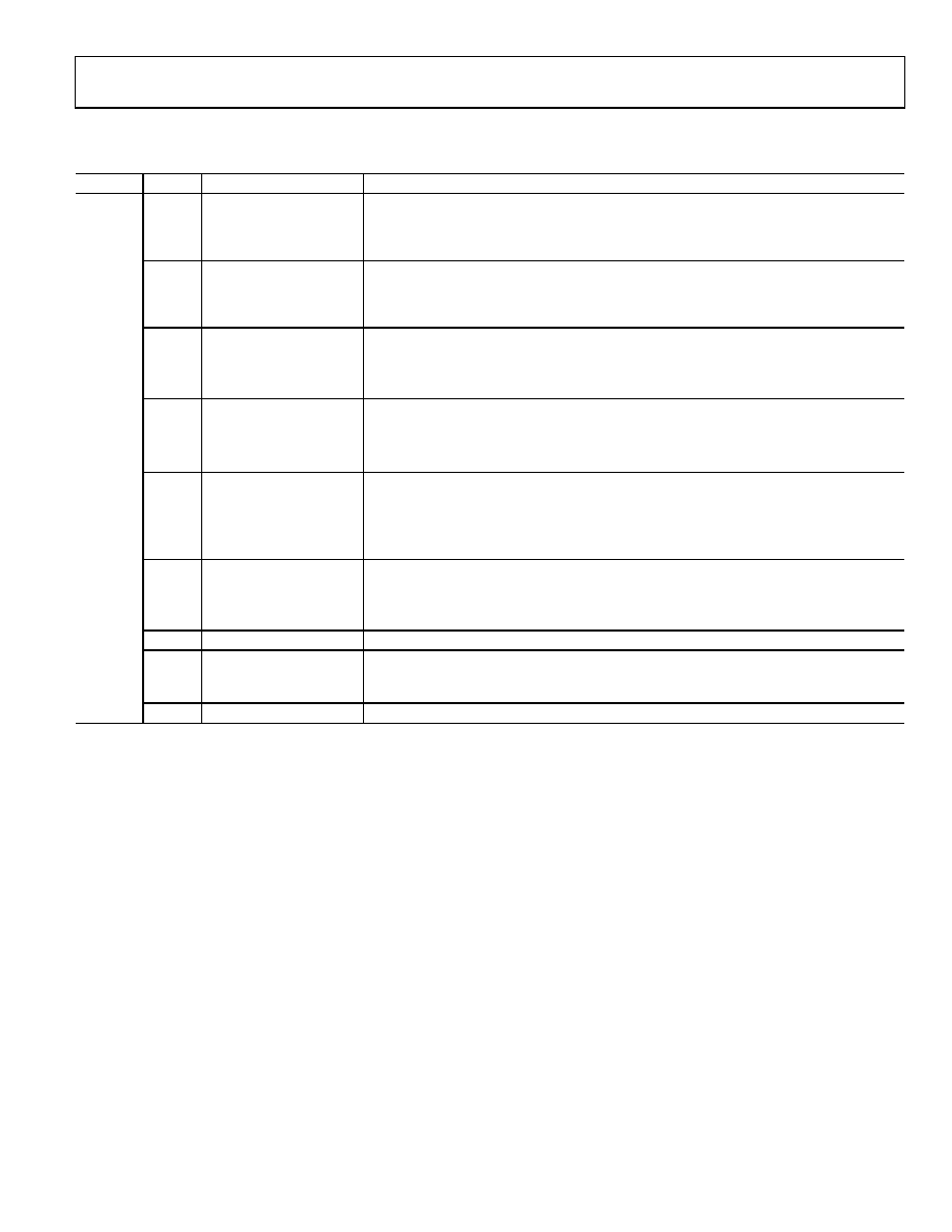
The data synchronization control register (DSCR) comprises two bytes located at Address 0x02.
Table 12. Data Synchronization Control Register (DSCR)
Address
Bit
Name
Description
0x02
[15:11]
DATACLK Delay [4:0]
Controls the amount of delay applied to the output data clock signal. The minimum delay
corresponds to the 00000 state, and the maximum delay corresponds to the 11111 state.
The minimum delay is 0.7 ns and the maximum delay is 6.5 ns. The incremental delay is
190 ps and corresponds to an incremental change in the data clock delay bits.
[10:7]
Data Timing Margin [3:0]
The data timing margin bits control the amount of delay applied to the data and clock
signals used for checking setup and hold times, respectively, on the input data ports, with
respect to the internal data assembler clock. The minimum delay corresponds to the 0000
state, and the maximum delay corresponds to the 1111 state. The delays are 190 ps.
[6]
LVDS data clock enable
0: Default. When the LVDS data clock enable bit is cleared, the SYNC_O+ and SYNC_O
LVDS pad cells are driven by the multichip synchronization logic.
1: When the LVDS data clock enable bit is set, the SYNC_O+ and SYNC_O LVDS pad cells
are driven by the signal that drives the CMOS DATACLK output pad.
[5]
DATACLK invert
0: Default. When the data clock invert bit is cleared, the DATACLK signal is in phase with
the clock that samples the data into the part.
1: When the DATACLK invert bit is set, the DATACLK signal is inverted from the clock that
samples the data into the part.
[4]
DATACLK delay enable
0: Default. When the DATACLK delay enable bit is cleared, the data port input
synchronization function is effectively inactive and the delay is bypassed.
1: When the DATACLK delay enable bit is set, the data port input synchronization function
is active and controlled by the data delay mode bits. The data output clock is routed
through the delay cell.
[3]
Data timing mode
Determines the timing optimization mode. See the Optimizing the Data Input Timing
section for details.
0: Manual timing optimization mode
1: Automatic timing optimization mode
[2]
Set high
This bit should always be set high.
[1]
Data sync polarity
0: Default. The digital input data sampling edge is aligned with the falling edge of DCI.
1: The digital input data sampling edge is aligned with the rising edge of DCI.
Used only in slave mode (see the MSCR register, Address 0x03, Bit 16).
[0]
Reserved
Reserved for future use.
相关PDF资料 |
PDF描述 |
|---|---|
| HFA1135IBZ | IC OPAMP CFA 360MHZ LP 8-SOIC |
| LTC2754BIUKG-16#TRPBF | IC DAC 16BIT QUAD IOUT 52-QFN |
| HA3-5020-5Z | IC AMP VIDEO CFA 100MHZ 8-DIP |
| HFA1105IBZ | IC OPAMP CFA 330MHZ LP 8-SOIC |
| VI-B1N-MU | CONVERTER MOD DC/DC 18.5V 200W |
相关代理商/技术参数 |
参数描述 |
|---|---|
| AD9785-DPG2-EBZ | 功能描述:BOARD EVALUATION FOR AD9785 RoHS:是 类别:编程器,开发系统 >> 评估板 - 数模转换器 (DAC) 系列:TxDAC® 产品培训模块:Lead (SnPb) Finish for COTS Obsolescence Mitigation Program 标准包装:1 系列:- DAC 的数量:4 位数:12 采样率(每秒):- 数据接口:串行,SPI? 设置时间:3µs DAC 型:电流/电压 工作温度:-40°C ~ 85°C 已供物品:板 已用 IC / 零件:MAX5581 |
| AD9785-EBZ | 制造商:Analog Devices 功能描述:Evaluation Board For AD9785 制造商:Analog Devices 功能描述:DUAL 12B, 1GSPS D-A CONVERTER - Bulk 制造商:Analog Devices 功能描述:Digital to Analog Eval. Board |
| AD9786 | 制造商:AD 制造商全称:Analog Devices 功能描述:16-Bit, 200 MSPS/500 MSPS TxDAC+ with 2】/4】/8】 Interpolation and Signal Processing |
| AD9786BSV | 制造商:Analog Devices 功能描述:DAC 1-CH Interpolation Filter 16-bit 80-Pin TQFP EP 制造商:Analog Devices 功能描述:IC 16BIT DAC SMD 9786 TQFP80 |
| AD9786BSVRL | 制造商:Analog Devices 功能描述:DAC 1-CH Interpolation Filter 16-bit 80-Pin TQFP EP T/R |
发布紧急采购,3分钟左右您将得到回复。