- 您现在的位置:买卖IC网 > PDF目录10978 > AD9832BRUZ-REEL (Analog Devices Inc)IC DDS 10BIT 25MHZ CMOS 16TSSOP PDF资料下载
参数资料
| 型号: | AD9832BRUZ-REEL |
| 厂商: | Analog Devices Inc |
| 文件页数: | 11/28页 |
| 文件大小: | 0K |
| 描述: | IC DDS 10BIT 25MHZ CMOS 16TSSOP |
| 产品培训模块: | Direct Digital Synthesis Tutorial Series (1 of 7): Introduction Direct Digital Synthesizer Tutorial Series (7 of 7): DDS in Action Direct Digital Synthesis Tutorial Series (3 of 7): Angle to Amplitude Converter Direct Digital Synthesis Tutorial Series (6 of 7): SINC Envelope Correction Direct Digital Synthesis Tutorial Series (4 of 7): Digital-to-Analog Converter Direct Digital Synthesis Tutorial Series (2 of 7): The Accumulator |
| 标准包装: | 2,500 |
| 分辨率(位): | 10 b |
| 主 fclk: | 25MHz |
| 调节字宽(位): | 32 b |
| 电源电压: | 2.97 V ~ 5.5 V |
| 工作温度: | -40°C ~ 85°C |
| 安装类型: | 表面贴装 |
| 封装/外壳: | 16-TSSOP(0.173",4.40mm 宽) |
| 供应商设备封装: | 16-TSSOP |
| 包装: | 带卷 (TR) |
第1页第2页第3页第4页第5页第6页第7页第8页第9页第10页当前第11页第12页第13页第14页第15页第16页第17页第18页第19页第20页第21页第22页第23页第24页第25页第26页第27页第28页
Data Sheet
AD9832
Rev. E | Page 19 of 28
APPLICATIONS INFORMATION
The AD9832 contains functions that make it suitable for
modulation applications. The part can be used to perform
simple modulation, such as FSK, and more complex modulation
schemes, such as GMSK and QPSK, can also be implemented
using the AD9832. In an FSK application, the two frequency
registers of the AD9832 are loaded with different values; one
frequency represents the space frequency while the other represents
the mark frequency. The digital data stream is fed to the FSELECT
pin, which causes the AD9832 to modulate the carrier frequency
between the two values.
The AD9832 has four phase registers; this enables the part to
perform PSK. With phase shift keying, the carrier frequency is
phase shifted, the phase being altered by an amount which is
related to the bit stream being input to the modulator. The
presence of four shift registers eases the interaction needed
between the DSP and the AD9832.
The AD9832 is also suitable for signal generator applications.
With its low current consumption, the part is suitable for
applications where it can be used as a local oscillator. In addition,
the part is fully specified for operation with a 3.3 V ± 10%
power supply. Therefore, in portable applications where current
consumption is an important issue, the AD9832 is perfect.
GROUNDING AND LAYOUT
The printed circuit board (PCB) that houses the AD9832
should be designed so that the analog and digital sections are
separated and confined to certain areas of the board. This
facilitates the use of ground planes that can be easily separated.
A minimum etch technique is generally best for ground planes
because it gives the best shielding. Digital and analog ground
planes should only be joined in one place. If the AD9832 is the
only device requiring an AGND-to-DGND connection, the
ground planes should be connected at the AGND and DGND
pins of the AD9832. If the AD9832 is in a system where multiple
devices require AGND-to-DGND connections, the connection
should be made at one point only, a star ground point that
should be established as close as possible to the AD9832.
Avoid running digital lines under the device as these couple
noise onto the die. The analog ground plane should be allowed
to run under the AD9832 to avoid noise coupling. The power
supply lines to the AD9832 should use as large a track as possible
to provide low impedance paths and reduce the effects of glitches
on the power supply line. Fast switching signals, such as clocks,
should be shielded with digital ground to avoid radiating noise
to other sections of the board. Avoid crossover of digital and analog
signals. Traces on opposite sides of the board should run at right
angles to each other, which reduces the effects of feedthrough
through the board. A microstrip technique is by far the best,
but it is not always possible with a double-sided board. In this
technique, the component side of the board is dedicated to
ground planes, while signals are placed on the other side.
Good decoupling is important. The analog and digital supplies
to the AD9832 are independent and separately pinned out to
minimize coupling between analog and digital sections of the
device. All analog and digital supplies should be decoupled to
AGND and DGND, respectively, with 0.1 F ceramic capacitors
in parallel with 10 F tantalum capacitors. To achieve the best
from the decoupling capacitors, they should be placed as close
as possible to the device, ideally right up against the device. In
systems where a common supply is used to drive both the AVDD
and DVDD of the AD9832, it is recommended that the AVDD
supply of the system be used. This supply should have the
recommended analog supply decoupling between the AVDD
pins of the AD9832 and AGND and the recommended digital
supply decoupling capacitors between the DVDD pins and DGND.
INTERFACING THE AD9832 TO MICROPROCESSORS
The AD9832 has a standard serial interface that allows the part
to interface directly with several microprocessors. The device
uses an external serial clock to write the data/control information
into the device. The serial clock can have a frequency of 20 MHz
maximum. The serial clock can be continuous, or it can idle
high or low between write operations. When data/control
information is being written to the AD9832, FSYNC is taken
low and held low while the 16 bits of data are being written into
the AD9832. The FSYNC signal frames the 16 bits of information
being loaded into the AD9832.
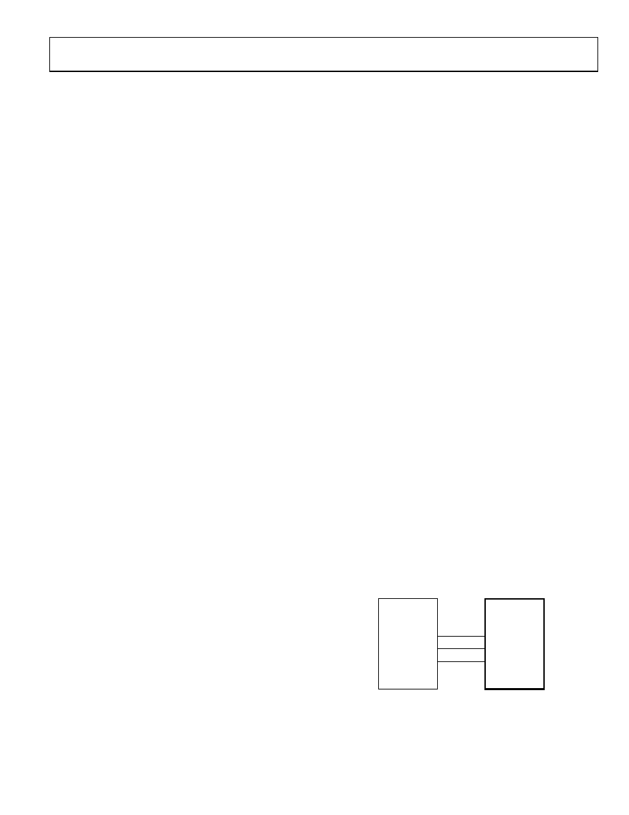
AD9832 TO ADSP-2101 INTERFACE
Figure 28 shows the serial interface between the AD9832 and
the ADSP-2101. The ADSP-2101 should be set up to operate
in SPORT transmit alternate framing mode (TFSW = 1). The
ADSP-2101 is programmed through the SPORT control register
and should be configured as follows: internal clock operation
(ISCLK = 1), active low framing (INVTFS = 1), 16-bit word
length (SLEN = 15), internal frame sync signal (ITFS = 1),
and a frame sync for each write operation (TFSR = 1) must
be generated. Transmission is initiated by writing a word to the
Tx register after SPORT is enabled. The data is clocked out on
each rising edge of the serial clock and clocked into the AD9832
on the SCLK falling edge.
AD9832*
FSYNC
SDATA
SCLK
ADSP-2101*
TFS
DT
SCLK
*ADDITIONAL PINS OMITTED FOR CLARITY.
09090-
028
Figure 28. ADSP-2101 to AD9832 Interface
相关PDF资料 |
PDF描述 |
|---|---|
| VE-B1H-IX-B1 | CONVERTER MOD DC/DC 52V 75W |
| AD9834BRUZ-REEL7 | IC DDS 10BIT 50MHZ LP 20TSSOP |
| VE-B1H-IW-B1 | CONVERTER MOD DC/DC 52V 100W |
| VE-B1F-IX-B1 | CONVERTER MOD DC/DC 72V 75W |
| MCF51AC256BCPUE | MCU 32BIT 256K FLASH 64-LQFP |
相关代理商/技术参数 |
参数描述 |
|---|---|
| AD9832BRUZ-REEL7 | 功能描述:IC DDS 10BIT 25MHZ CMOS 16TSSOP RoHS:是 类别:集成电路 (IC) >> 接口 - 直接数字合成 (DDS) 系列:- 产品变化通告:Product Discontinuance 27/Oct/2011 标准包装:2,500 系列:- 分辨率(位):10 b 主 fclk:25MHz 调节字宽(位):32 b 电源电压:2.97 V ~ 5.5 V 工作温度:-40°C ~ 85°C 安装类型:表面贴装 封装/外壳:16-TSSOP(0.173",4.40mm 宽) 供应商设备封装:16-TSSOP 包装:带卷 (TR) |
| AD9833 | 制造商:AD 制造商全称:Analog Devices 功能描述:+2.5 V to +5.5 V, 25 MHz Low Power CMOS Complete DDS |
| AD9833BRM | 功能描述:IC WAVEFORM GEN PROG 10-MSOP RoHS:否 类别:集成电路 (IC) >> 接口 - 直接数字合成 (DDS) 系列:- 产品变化通告:Product Discontinuance 27/Oct/2011 标准包装:2,500 系列:- 分辨率(位):10 b 主 fclk:25MHz 调节字宽(位):32 b 电源电压:2.97 V ~ 5.5 V 工作温度:-40°C ~ 85°C 安装类型:表面贴装 封装/外壳:16-TSSOP(0.173",4.40mm 宽) 供应商设备封装:16-TSSOP 包装:带卷 (TR) |
| AD9833BRM-REEL | 制造商:Analog Devices 功能描述:Direct Digital Synthesizer 25MHz 1-DAC 10-Bit Serial 10-Pin MSOP T/R 制造商:Analog Devices 功能描述:PROGRAMMABLE WAVEFORM GENERATOR 10MSOP - Tape and Reel |
| AD9833BRM-REEL7 | 功能描述:IC WAVEFORM GEN PROG 10-MSOP RoHS:否 类别:集成电路 (IC) >> 接口 - 直接数字合成 (DDS) 系列:- 产品变化通告:Product Discontinuance 27/Oct/2011 标准包装:2,500 系列:- 分辨率(位):10 b 主 fclk:25MHz 调节字宽(位):32 b 电源电压:2.97 V ~ 5.5 V 工作温度:-40°C ~ 85°C 安装类型:表面贴装 封装/外壳:16-TSSOP(0.173",4.40mm 宽) 供应商设备封装:16-TSSOP 包装:带卷 (TR) |
发布紧急采购,3分钟左右您将得到回复。