- 您现在的位置:买卖IC网 > PDF目录10978 > AD9832BRUZ-REEL (Analog Devices Inc)IC DDS 10BIT 25MHZ CMOS 16TSSOP PDF资料下载
参数资料
| 型号: | AD9832BRUZ-REEL |
| 厂商: | Analog Devices Inc |
| 文件页数: | 6/28页 |
| 文件大小: | 0K |
| 描述: | IC DDS 10BIT 25MHZ CMOS 16TSSOP |
| 产品培训模块: | Direct Digital Synthesis Tutorial Series (1 of 7): Introduction Direct Digital Synthesizer Tutorial Series (7 of 7): DDS in Action Direct Digital Synthesis Tutorial Series (3 of 7): Angle to Amplitude Converter Direct Digital Synthesis Tutorial Series (6 of 7): SINC Envelope Correction Direct Digital Synthesis Tutorial Series (4 of 7): Digital-to-Analog Converter Direct Digital Synthesis Tutorial Series (2 of 7): The Accumulator |
| 标准包装: | 2,500 |
| 分辨率(位): | 10 b |
| 主 fclk: | 25MHz |
| 调节字宽(位): | 32 b |
| 电源电压: | 2.97 V ~ 5.5 V |
| 工作温度: | -40°C ~ 85°C |
| 安装类型: | 表面贴装 |
| 封装/外壳: | 16-TSSOP(0.173",4.40mm 宽) |
| 供应商设备封装: | 16-TSSOP |
| 包装: | 带卷 (TR) |
第1页第2页第3页第4页第5页当前第6页第7页第8页第9页第10页第11页第12页第13页第14页第15页第16页第17页第18页第19页第20页第21页第22页第23页第24页第25页第26页第27页第28页
AD9832
Data Sheet
Rev. E | Page 14 of 28
FUNCTIONAL DESCRIPTION
SERIAL INTERFACE
The AD9832 has a serial interface, with 16 bits being loaded
during each write cycle. SCLK, SDATA, and FSYNC are used to
load the word into the AD9832.
When FSYNC is taken low, the AD9832 is informed that a word
is being written to the device. The first bit is read into the device
on the next SCLK falling edge with the remaining bits being read
into the device on the subsequent SCLK falling edges. FSYNC
frames the 16 bits; therefore, when 16 SCLK falling edges have
occurred, FSYNC should be taken high again. The SCLK can be
continuous, or alternatively, the SCLK can idle high or low between
write operations.
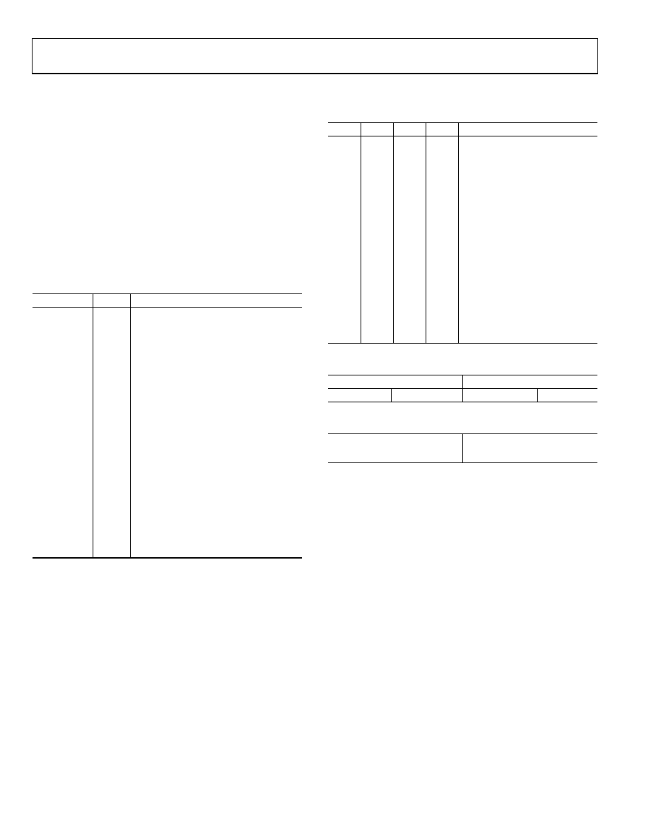
Table 5. Control Registers
Register
Size
Description
FREQ0 REG
32 bits
Frequency Register 0. This defines the
output frequency, when FSELECT = 0,
as a fraction of the MCLK frequency.
FREQ1 REG
32 bits
Frequency Register 1. This defines the
output frequency, when FSELECT = 1,
as a fraction of the MCLK frequency.
PHASE0 REG
12 bits
Phase Offset Register 0. When PSEL0 =
PSEL1 = 0, the contents of this register
are added to the output of the phase
accumulator.
PHASE1 REG
12 bits
Phase Offset Register 1. When PSEL0 = 1
and PSEL1 = 0, the contents of this
register are added to the output of the
phase accumulator.
PHASE2 REG
12 bits
Phase Offset Register 2. When PSEL0 = 0
and PSEL1 = 1, the contents of this
register are added to the output of the
phase accumulator.
PHASE3 REG
12 bits
Phase Offset Register 3. When PSEL0 =
PSEL1 = 1, the contents of this register
are added to the output of the phase
accumulator.
When writing to a frequency/phase register, the first four bits
identify whether a frequency or phase register is being written to,
the next four bits contain the address of the destination register,
while the 8 LSBs contain the data. Table 6 lists the addresses for
the phase/frequency registers, and Table 7 and Table 8 list the
data structure for each.
For an example on programming the AD9832, see the AN-621
application note, Programming the AD9832/AD9835, at
Table 6. Addressing the Registers
A3
A2
A1
A0
Destination Register
0
FREQ0 REG 8 L LSBs
0
1
FREQ0 REG 8 H LSBs
0
1
0
FREQ0 REG 8 L MSBs
0
1
FREQ0 REG 8 H MSBs
0
1
0
FREQ1 REG 8 L LSBs
0
1
0
1
FREQ1 REG 8 H LSBs
0
1
0
FREQ1 REG 8 L MSBs
0
1
FREQ1 REG 8 H MSBs
1
0
PHASE0 REG 8 LSBs
1
0
1
PHASE0 REG 8 MSBs
1
0
1
0
PHASE1 REG 8 LSBs
1
0
1
PHASE1 REG 8 MSBs
1
0
PHASE2 REG 8 LSBs
1
0
1
PHASE2 REG 8 MSBs
1
0
PHASE3 REG 8 LSBs
1
PHASE3 REG 8 MSBs
Table 7. 32-Bit Frequency Word
16 MSBs
16 LSBs
8 H MSBs
8 L MSBs
8 H LSBs
8 L LSBs
Table 8. 12-Bit Frequency Word
4 MSBs (The 4 MSBs of the
8-Bit Word Loaded = 0)
8 LSBs
DIRECT DATA TRANSFER AND DEFERRED DATA
TRANSFER
Within the AD9832, 16-bit transfers are used when loading the
destination frequency/phase register. There are two modes for
loading a register, direct data transfer and a deferred data transfer.
With a deferred data transfer, the 8-bit word is loaded into the
defer register (8 LSBs or 8 MSBs). However, this data is not
loaded into the 16-bit data register; therefore, the destination
register is not updated. With a direct data transfer, the 8-bit word is
loaded into the appropriate defer register (8 LSBs or 8 MSBs).
Immediately following the loading of the defer register, the
contents of the complete defer register are loaded into the 16-bit
data register and the destination register is loaded on the next
MCLK rising edge. When a destination register is addressed, a
deferred transfer is needed first followed by a direct transfer.
When all 16 bits of the defer register contain relevant data, the
destination register can then be updated using 8-bit loading
rather than 16-bit loading, that is, direct data transfers can be
used. For example, after a new 16-bit word has been loaded to a
destination register, the defer register will also contain this
word. If the next write instruction is to the same destination
register, the user can use direct data transfers immediately.
相关PDF资料 |
PDF描述 |
|---|---|
| VE-B1H-IX-B1 | CONVERTER MOD DC/DC 52V 75W |
| AD9834BRUZ-REEL7 | IC DDS 10BIT 50MHZ LP 20TSSOP |
| VE-B1H-IW-B1 | CONVERTER MOD DC/DC 52V 100W |
| VE-B1F-IX-B1 | CONVERTER MOD DC/DC 72V 75W |
| MCF51AC256BCPUE | MCU 32BIT 256K FLASH 64-LQFP |
相关代理商/技术参数 |
参数描述 |
|---|---|
| AD9832BRUZ-REEL7 | 功能描述:IC DDS 10BIT 25MHZ CMOS 16TSSOP RoHS:是 类别:集成电路 (IC) >> 接口 - 直接数字合成 (DDS) 系列:- 产品变化通告:Product Discontinuance 27/Oct/2011 标准包装:2,500 系列:- 分辨率(位):10 b 主 fclk:25MHz 调节字宽(位):32 b 电源电压:2.97 V ~ 5.5 V 工作温度:-40°C ~ 85°C 安装类型:表面贴装 封装/外壳:16-TSSOP(0.173",4.40mm 宽) 供应商设备封装:16-TSSOP 包装:带卷 (TR) |
| AD9833 | 制造商:AD 制造商全称:Analog Devices 功能描述:+2.5 V to +5.5 V, 25 MHz Low Power CMOS Complete DDS |
| AD9833BRM | 功能描述:IC WAVEFORM GEN PROG 10-MSOP RoHS:否 类别:集成电路 (IC) >> 接口 - 直接数字合成 (DDS) 系列:- 产品变化通告:Product Discontinuance 27/Oct/2011 标准包装:2,500 系列:- 分辨率(位):10 b 主 fclk:25MHz 调节字宽(位):32 b 电源电压:2.97 V ~ 5.5 V 工作温度:-40°C ~ 85°C 安装类型:表面贴装 封装/外壳:16-TSSOP(0.173",4.40mm 宽) 供应商设备封装:16-TSSOP 包装:带卷 (TR) |
| AD9833BRM-REEL | 制造商:Analog Devices 功能描述:Direct Digital Synthesizer 25MHz 1-DAC 10-Bit Serial 10-Pin MSOP T/R 制造商:Analog Devices 功能描述:PROGRAMMABLE WAVEFORM GENERATOR 10MSOP - Tape and Reel |
| AD9833BRM-REEL7 | 功能描述:IC WAVEFORM GEN PROG 10-MSOP RoHS:否 类别:集成电路 (IC) >> 接口 - 直接数字合成 (DDS) 系列:- 产品变化通告:Product Discontinuance 27/Oct/2011 标准包装:2,500 系列:- 分辨率(位):10 b 主 fclk:25MHz 调节字宽(位):32 b 电源电压:2.97 V ~ 5.5 V 工作温度:-40°C ~ 85°C 安装类型:表面贴装 封装/外壳:16-TSSOP(0.173",4.40mm 宽) 供应商设备封装:16-TSSOP 包装:带卷 (TR) |
发布紧急采购,3分钟左右您将得到回复。