- 您现在的位置:买卖IC网 > PDF目录10978 > AD9837ACPZ-RL (Analog Devices Inc)IC WAVEFORM GEN PROG 10LFCSP PDF资料下载
参数资料
| 型号: | AD9837ACPZ-RL |
| 厂商: | Analog Devices Inc |
| 文件页数: | 8/28页 |
| 文件大小: | 0K |
| 描述: | IC WAVEFORM GEN PROG 10LFCSP |
| 产品培训模块: | Direct Digital Synthesis Tutorial Series (1 of 7): Introduction Direct Digital Synthesizer Tutorial Series (7 of 7): DDS in Action Direct Digital Synthesis Tutorial Series (3 of 7): Angle to Amplitude Converter Direct Digital Synthesis Tutorial Series (6 of 7): SINC Envelope Correction Direct Digital Synthesis Tutorial Series (4 of 7): Digital-to-Analog Converter Direct Digital Synthesis Tutorial Series (2 of 7): The Accumulator |
| 标准包装: | 5,000 |
| 分辨率(位): | 10 b |
| 主 fclk: | 5MHz |
| 调节字宽(位): | 28 b |
| 电源电压: | 2.3 V ~ 5.5 V |
| 工作温度: | -40°C ~ 125°C |
| 安装类型: | 表面贴装 |
| 封装/外壳: | 10-WFDFN 裸露焊盘,CSP |
| 供应商设备封装: | 10-LFCSP-WD(3x3) |
| 包装: | 带卷 (TR) |
第1页第2页第3页第4页第5页第6页第7页当前第8页第9页第10页第11页第12页第13页第14页第15页第16页第17页第18页第19页第20页第21页第22页第23页第24页第25页第26页第27页第28页
AD9837
Data Sheet
Rev. A | Page 16 of 28
RESET FUNCTION
The reset function resets the appropriate internal registers to 0
to provide an analog output of midscale. A reset does not reset
the phase, frequency, or control registers. When the AD9837 is
powered up, the part should be reset (see the Powering Up the
AD9837 section). To reset the AD9837, set the RESET bit to 1.
To take the part out of reset, set the bit to 0. A signal appears at
the DAC output seven or eight MCLK cycles after the RESET
bit is set to 0.
Table 14. Applying the Reset Function
RESET Bit
Result
0
No reset applied
1
Internal registers reset
SLEEP FUNCTION
Sections of the AD9837 that are not in use can be powered
down to minimize power consumption by using the sleep
function. The parts of the chip that can be powered down are
the internal clock and the DAC. The bits required for the sleep
function are shown in Table 15.
Table 15. Applying the Sleep Function
SLEEP1 Bit
SLEEP12 Bit
Result
0
No power-down
0
1
DAC powered down
1
0
Internal clock disabled
1
DAC powered down and
internal clock disabled
DAC Powered Down
When the AD9837 is used to output the MSB of the DAC data
only, the DAC is not required. The DAC can be powered down
using the SLEEP12 bit to reduce power consumption.
Internal Clock Disabled
When the internal clock of the AD9837 is disabled, the DAC
output remains at its present value because the NCO is no
longer accumulating. New frequency, phase, and control words
can be written to the part when the SLEEP1 control bit is active.
Because the synchronizing clock (FSYNC) remains active, the
selected frequency and phase registers can also be changed using
the control bits. Setting the SLEEP1 bit to 0 enables the MCLK.
Any changes made to the registers while SLEEP1 was active are
observed at the output after a latency period (see the Latency
Period section).
VOUT PIN
The AD9837 offers a variety of outputs from the chip, all of
which are available from the VOUT pin. The available outputs
are the MSB of the DAC data, a sinusoidal output, or a triangle
output.
The OPBITEN and MODE bits (Bit D5 and Bit D1 in the
control register) are used to determine the output that is
available from the AD9837 (see Table 16).
Table 16. Outputs from the VOUT Pin
OPBITEN Bit
MODE Bit
DIV2 Bit
VOUT Pin Output
0
X
Sinusoid
0
1
X
Triangle
1
0
DAC data MSB/2
1
0
1
DAC data MSB
1
X
Reserved
MSB of the DAC Data
The MSB of the DAC data can be output from the AD9837. By
setting the OPBITEN bit (Bit D5) to 1, the MSB of the DAC data
is available at the VOUT pin. This is useful as a coarse clock
source. This square wave can also be divided by 2 before being
output. The DIV2 bit (Bit D3) in the control register controls
the frequency of this output from the VOUT pin.
Sinusoidal Output
The SIN ROM converts the phase information from the frequency
and phase registers into amplitude information, resulting in a
sinusoidal signal at the output. To obtain a sinusoidal output
from the VOUT pin, set the MODE bit (Bit D1) to 0 and the
OPBITEN bit (Bit D5) to 0.
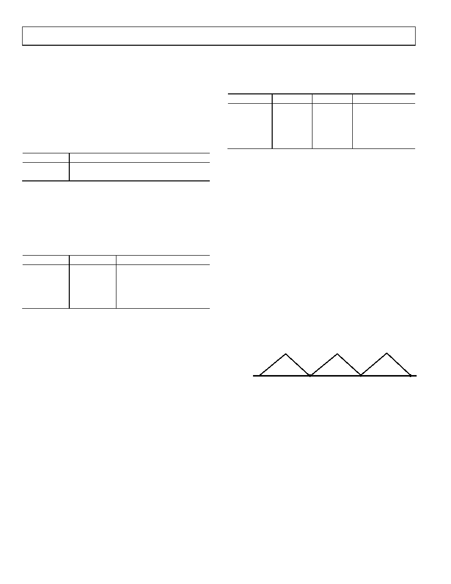
Triangle Output
The SIN ROM can be bypassed so that the truncated digital output
from the NCO is sent to the DAC. In this case, the output is no
longer sinusoidal. The DAC produces a 10-bit linear triangular
function (see Figure 21). To obtain a triangle output from the
VOUT pin, set the MODE bit (Bit D1) to 1 and the OPBITEN
bit (Bit D5) to 0.
VOUT MIN
VOUT MAX
2π
4π
6π
09070-
025
Figure 21. Triangle Output
POWERING UP THE AD9837
The flowchart in Figure 22 shows the operating routine for the
AD9837. When the AD9837 is powered up, the part should be
reset. This resets the appropriate internal registers to 0 to provide
an analog output of midscale. To avoid spurious DAC outputs
during AD9837 initialization, the RESET bit should be set to 1
until the part is ready to begin generating an output.
A reset does not reset the phase, frequency, or control registers.
These registers will contain invalid data and, therefore, should
be set to known values by the user. The RESET bit should then
be set to 0 to begin generating an output. The data appears on
the DAC output seven or eight MCLK cycles after the RESET
bit is set to 0.
相关PDF资料 |
PDF描述 |
|---|---|
| VE-2W3-IY-F4 | CONVERTER MOD DC/DC 24V 50W |
| VE-2W2-IY-F3 | CONVERTER MOD DC/DC 15V 50W |
| VE-2W1-IY-F2 | CONVERTER MOD DC/DC 12V 50W |
| VE-2W0-IY-F3 | CONVERTER MOD DC/DC 5V 50W |
| VE-21X-IY-F3 | CONVERTER MOD DC/DC 5.2V 50W |
相关代理商/技术参数 |
参数描述 |
|---|---|
| AD9837ACPZ-RL7 | 功能描述:IC WAVEFORM GEN PROG 10LFCSP RoHS:是 类别:集成电路 (IC) >> 接口 - 直接数字合成 (DDS) 系列:- 产品变化通告:Product Discontinuance 27/Oct/2011 标准包装:2,500 系列:- 分辨率(位):10 b 主 fclk:25MHz 调节字宽(位):32 b 电源电压:2.97 V ~ 5.5 V 工作温度:-40°C ~ 85°C 安装类型:表面贴装 封装/外壳:16-TSSOP(0.173",4.40mm 宽) 供应商设备封装:16-TSSOP 包装:带卷 (TR) |
| AD9837BCPZ-RL | 功能描述:IC WAVEFORM GEN PROG 10LFCSP RoHS:是 类别:集成电路 (IC) >> 接口 - 直接数字合成 (DDS) 系列:- 产品变化通告:Product Discontinuance 27/Oct/2011 标准包装:2,500 系列:- 分辨率(位):10 b 主 fclk:25MHz 调节字宽(位):32 b 电源电压:2.97 V ~ 5.5 V 工作温度:-40°C ~ 85°C 安装类型:表面贴装 封装/外壳:16-TSSOP(0.173",4.40mm 宽) 供应商设备封装:16-TSSOP 包装:带卷 (TR) |
| AD9837BCPZ-RL7 | 功能描述:IC WAVEFORM GEN PROG 10LFCSP RoHS:是 类别:集成电路 (IC) >> 接口 - 直接数字合成 (DDS) 系列:- 产品变化通告:Product Discontinuance 27/Oct/2011 标准包装:2,500 系列:- 分辨率(位):10 b 主 fclk:25MHz 调节字宽(位):32 b 电源电压:2.97 V ~ 5.5 V 工作温度:-40°C ~ 85°C 安装类型:表面贴装 封装/外壳:16-TSSOP(0.173",4.40mm 宽) 供应商设备封装:16-TSSOP 包装:带卷 (TR) |
| AD9838 | 制造商:AD 制造商全称:Analog Devices 功能描述:11 mW Power, 2.3 V to 5.5 V, Complete DDS Power-down option |
| AD9838ACPZ-RL | 功能描述:IC DDS 16MHZ LOW PWR 20LFCSP RoHS:是 类别:集成电路 (IC) >> 接口 - 直接数字合成 (DDS) 系列:- 产品变化通告:Product Discontinuance 27/Oct/2011 标准包装:2,500 系列:- 分辨率(位):10 b 主 fclk:25MHz 调节字宽(位):32 b 电源电压:2.97 V ~ 5.5 V 工作温度:-40°C ~ 85°C 安装类型:表面贴装 封装/外壳:16-TSSOP(0.173",4.40mm 宽) 供应商设备封装:16-TSSOP 包装:带卷 (TR) |
发布紧急采购,3分钟左右您将得到回复。