- 您现在的位置:买卖IC网 > PDF目录16463 > AD9854/PCBZ (Analog Devices Inc)BOARD EVAL FOR AD9854 PDF资料下载
参数资料
| 型号: | AD9854/PCBZ |
| 厂商: | Analog Devices Inc |
| 文件页数: | 18/52页 |
| 文件大小: | 0K |
| 描述: | BOARD EVAL FOR AD9854 |
| 产品培训模块: | Direct Digital Synthesis Tutorial Series (1 of 7): Introduction Direct Digital Synthesizer Tutorial Series (7 of 7): DDS in Action Direct Digital Synthesis Tutorial Series (3 of 7): Angle to Amplitude Converter Direct Digital Synthesis Tutorial Series (6 of 7): SINC Envelope Correction Direct Digital Synthesis Tutorial Series (4 of 7): Digital-to-Analog Converter Direct Digital Synthesis Tutorial Series (2 of 7): The Accumulator |
| 设计资源: | AD9854 Eval Brd Schematic AD9854 Eval Brd BOM |
| 标准包装: | 1 |
| 系列: | AgileRF™ |
| 主要目的: | 计时,直接数字合成(DDS) |
| 已用 IC / 零件: | AD9854 |
| 已供物品: | 板 |
| 相关产品: | AD9854ASTZ-ND - IC DDS QUADRATURE CMOS 80-LQFP |
第1页第2页第3页第4页第5页第6页第7页第8页第9页第10页第11页第12页第13页第14页第15页第16页第17页当前第18页第19页第20页第21页第22页第23页第24页第25页第26页第27页第28页第29页第30页第31页第32页第33页第34页第35页第36页第37页第38页第39页第40页第41页第42页第43页第44页第45页第46页第47页第48页第49页第50页第51页第52页
AD9854
Rev. E | Page 25 of 52
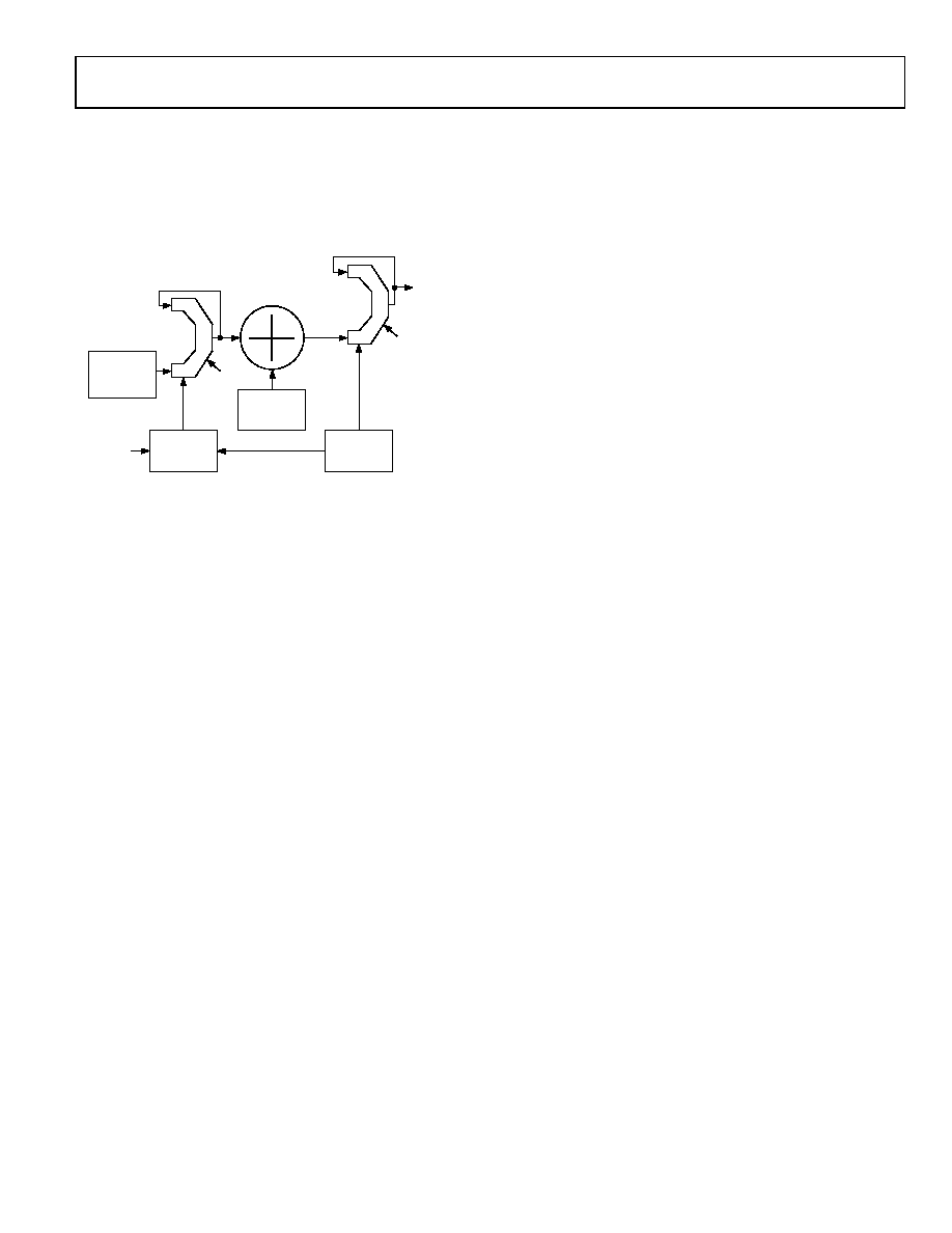
The AD9854 permits precise, internally generated linear, or
externally programmed nonlinear, pulsed or continuous FM
over the complete frequency range, duration, frequency
resolution, and sweep direction(s). All of these are user
programmable. Figure 44 shows a block diagram of the FM
chirp components.
20-BIT
RAMP RATE
CLOCK
48-BIT DELTA
FREQUENCY
WORD (TWOS
COMPLEMENT)
FREQUENCY
ACCUMULATOR
PHASE
ACCUMULATOR
OUT
ADDER
SYSTEM
CLOCK
CLR ACC2
CLR ACC1
FREQUENCY
TUNING
WORD 1
HOLD
0063
6-
044
Figure 44. FM Chirp Components
Basic FM Chirp Programming Steps
1.
Program a start frequency into Frequency Tuning Word 1
(FTW1) at Parallel Register Address 4 hex to Parallel Register
Address 9 hex.
2.
Program the frequency step resolution into the 48-bit,
twos complement delta frequency word (Parallel Register
Address 10 hex to Parallel Register Address 15 hex).
3.
Program the rate of change (time at each frequency) into
the 20-bit ramp rate clock (Parallel Register Address 1A hex
to Parallel Register Address 1C hex).
When programming is complete, an I/O update pulse at Pin 20
engages the program commands.
The necessity for a twos complement delta frequency word is to
define the direction in which the FM chirp moves. If the 48-bit
delta frequency word is negative (MSB is high), the incremental
frequency changes are in a negative direction from FTW1. If the
48-bit word is positive (MSB is low), the incremental frequency
changes are in a positive direction from FTW1.
It is important to note that FTW1 is only a starting point for FM
chirp. There is no built-in restraint requiring a return to FTW1.
Once the FM chirp begins, it is free to move (under program
control) within the Nyquist bandwidth (dc to one-half the system
clock). However, instant return to FTW1 can be easily achieved.
Two control bits (CLR ACC1 and CLR ACC2) are available
in the FM chirp mode that allow the return to the beginning
frequency, FTW1, or to 0 Hz. When the CLR ACC1 bit
(Register Address 1F hex) is set high, the 48-bit frequency
accumulator (ACC1) output is cleared with a retriggerable
one-shot pulse of one system clock duration. The 48-bit delta
frequency word input to the accumulator is unaffected by the
CLR ACC1 bit. If the CLR ACC1 bit is held high, a one-shot
pulse is delivered to the frequency accumulator (ACC1) on every
rising edge of the I/O update clock. The effect is to interrupt the
current chirp, reset the frequency to that programmed into FTW1,
and continue the chirp at the previously programmed rate and
direction. Clearing the output of the frequency accumulator in
the chirp mode is illustrated in Figure 45. Shown in the diagram
is the I/O update clock, which is either user supplied or internally
generated.
Alternatively, the CLR ACC2 control bit (Register Address 1F hex)
is available to clear both the frequency accumulator (ACC1)
and the phase accumulator (ACC2). When this bit is set high,
the output of the phase accumulator results in 0 Hz output from
the DDS. As long as this bit is set high, the frequency and phase
accumulators are cleared, resulting in 0 Hz output. To return to
the previous DDS operation, CLR ACC2 must be set to logic
low. This bit is useful in generating pulsed FM.
Figure 46 illustrates the effect of the CLR ACC2 bit on the DDS
output frequency. Note that reprogramming the registers while
the CLR ACC2 bit is high allows a new FTW1 frequency and
slope to be loaded.
Another function that is available only in chirp mode is the
HOLD pin (Pin 29). This function stops the clock signal to the
ramp rate counter, halting any further clocking pulses to
the frequency accumulator, ACC1. The effect is to halt the chirp
at the frequency existing just before the HOLD pin is pulled
high. When Pin 29 is returned low, the clock and chirp resumes.
During a hold condition, the user can change the programming
registers; however, the ramp rate counter must resume operation at
its previous rate until a count of 0 is obtained before a new ramp
rate count can be loaded. Figure 47 shows the effect of the hold
function on the DDS output frequency.
相关PDF资料 |
PDF描述 |
|---|---|
| LK2125R22K-T | INDUCTOR MULTILAYER .22UH 0805 |
| 6588719-2 | C/A MTRJ-LC DUP OFNR XG |
| M3UUK-2006R | IDC CABLE - MKS20K/MC20M/MKS20K |
| EEM30DTMI-S189 | CONN EDGECARD 60POS R/A .156 SLD |
| 6278033-3 | C/A MT-RJ/MT-RJ SM |
相关代理商/技术参数 |
参数描述 |
|---|---|
| AD9856 | 制造商:AD 制造商全称:Analog Devices 功能描述:CMOS 200 MHz Quadrature Digital Upconverter |
| AD9856/PCB | 制造商:Analog Devices 功能描述:Evaluation Board For Digital Up Converter 56 Pin LFCSP Ep 制造商:Analog Devices 功能描述:DGTL UP CNVRTR 56LFCSP - Bulk |
| AD9856AST | 制造商:Analog Devices 功能描述:Digital Up Converter 48-Pin LQFP Tray 制造商:Analog Devices 功能描述:IC MODULATOR DIGITAL |
| AD9856ASTZ | 功能描述:IC UPCONVERTER DGTL QUAD 48TQFP RoHS:是 类别:RF/IF 和 RFID >> RF 其它 IC 和模块 系列:AD9856 标准包装:100 系列:* |
| AD9857 | 制造商:AD 制造商全称:Analog Devices 功能描述:CMOS 200 MSPS 14-Bit Quadrature Digital Upconverter |
发布紧急采购,3分钟左右您将得到回复。