参数资料
| 型号: | AD9879BSZ |
| 厂商: | Analog Devices Inc |
| 文件页数: | 3/32页 |
| 文件大小: | 0K |
| 描述: | IC PROCESSOR FRONT END 100MQFP |
| 标准包装: | 1 |
| 位数: | 12 |
| 通道数: | 5 |
| 功率(瓦特): | 587mW |
| 电压 - 电源,模拟: | 3.3V |
| 电压 - 电源,数字: | 3.3V |
| 封装/外壳: | 100-BQFP |
| 供应商设备封装: | 100-MQFP(14x20) |
| 包装: | 托盘 |
第1页第2页当前第3页第4页第5页第6页第7页第8页第9页第10页第11页第12页第13页第14页第15页第16页第17页第18页第19页第20页第21页第22页第23页第24页第25页第26页第27页第28页第29页第30页第31页第32页
AD9879
Rev. A | Page 11 of 32
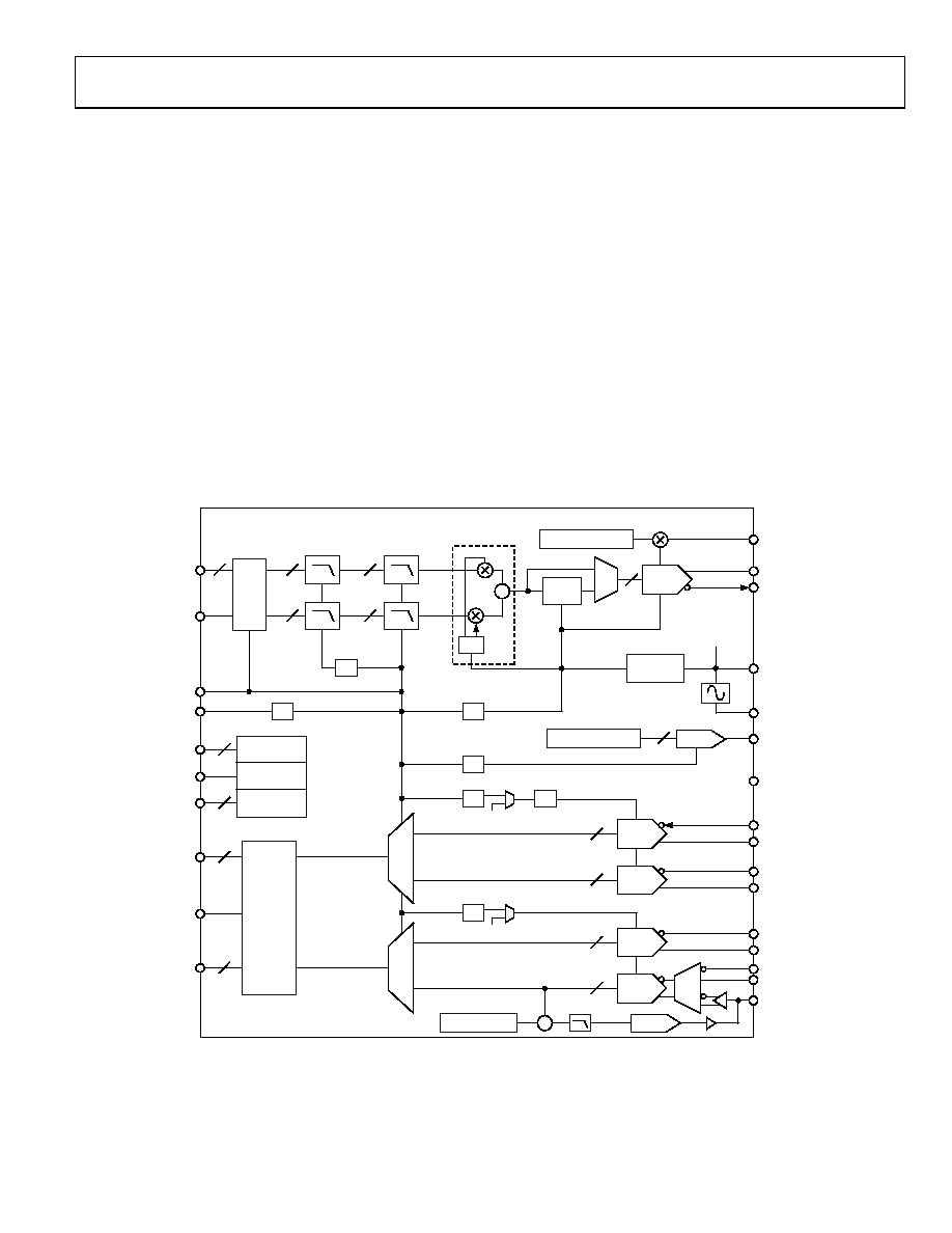
THEORY OF OPERATION
To gain a general understanding of the AD9879, refer to the
block diagram of the device architecture in Figure 3. The
device consists of a transmit path, receive path, and auxiliary
functions, such as a DPLL, a Σ-Δ DAC, a serial control port,
and a cable amplifier interface.
TRANSMIT PATH
The transmit path contains an interpolation filter, a complete
quadrature digital upconverter, an inverse sinc filter, and a
12-bit current output DAC. The maximum output current of
the DAC is set by an external resistor. The Tx output PGA
provides additional transmit signal level control.
The transmit path interpolation filter provides an upsampling
factor of 16 with an output signal bandwidth as high as
5.8 MHz. Carrier frequencies up to 65 MHz with 26 bits of
frequency tuning resolution can be generated by the direct
digital synthesizer (DDS).
The transmit DAC resolution is 12 bits and can run at sampling
rates as high as 232 MSPS. Analog output scaling from 0.0 dB
to 7.5 dB in 0.5 dB steps is available to preserve SNR when
reduced output levels are required.
DATA ASSEMBLER
The AD9879 data path operates on two 12-bit words, the I and
Q components, which compose a complex symbol. The data
assembler builds the 24-bit complex symbols from four
consecutive 6-bit nibbles read over the TxIQ[5:0] bus. The
nibbles are strobed synchronous to the master clock, MCLK,
into the data assembler. A high level on TxSYNC signals the
start of a transmit symbol. The first two nibbles of the symbol
form the I component, and the second two nibbles form the Q
component. Symbol components are assumed to be in twos
complement format. The timing of the interface is fully
described in the Transmit Timing section of this data sheet.
TXIQ
TXSYNC
MCLK
REFCLK
CA_PORT
PROFILE
SPORT
RXIQ[3:0]
RXSYNC
IF[11:0]
FSADJ
XTAL
OSCIN
Σ-_OUT
FLAG1
I INPUT
Q INPUT
IF10 INPUT
IF12 INPUT
VIDEO INPUT
6
3
12
10
7
12
AD9879
DATA
ASSEMBLER
QUADRATURE
MODULATOR
FIR LPF
CIC LPF
COS
SIN
(fIQCLK)
(fSYSCLK)
(fOSCIN)
(fMCLK)
DAC GAIN CONTROL
PLL
OSCIN
× M
DDS
MUX
CA
INTERFACE
PROFILE
SELECT
SERIAL
INTERFACE
12
4
÷4
SINC–1
MUX
DAC
IQ
IF
CLAMP LEVEL
ADC
MUX
DAC
÷2
÷8
÷4
÷2
12
(fOSCIN)
7
÷R
4
12
I
Q
RXPORT
TX
Σ- INPUT REGISTER
–
+
—
÷2
4
12
—
SINC–1
BYPASS
Σ-
02773-
003
Figure 3. Block Diagram
相关PDF资料 |
PDF描述 |
|---|---|
| AD9901KQ | IC PHASE/FREQ DISCRIMR 14-CDIP |
| AD9920ABBCZRL | IC PROCESSOR CCD 12BIT 105CSPBGA |
| AD9978BCPZRL | IC PROCESSOR CCD 14BIT 40-LFCSP |
| ADADC71KD | IC ADC 16BIT HIGH RES 32-CDIP |
| ADADC80-Z-12 | IC ADC 12BIT INTEGRATED 32-CDIP |
相关代理商/技术参数 |
参数描述 |
|---|---|
| AD9879BSZKL1 | 制造商:Rochester Electronics LLC 功能描述: 制造商:Analog Devices 功能描述: |
| AD9879-EB | 制造商:Analog Devices 功能描述:Evaluation Board For Mixed Signal Front End Set Top Box, Cable Modem 制造商:Analog Devices 功能描述:DEV TOOLS, MIXED SGNL FRONT END SET TOP , CBL MODEM - Bulk |
| AD9880 | 制造商:Analog Devices 功能描述:AUDIO PROCESSOR - Bulk |
| AD9880/PCB | 制造商:AD 制造商全称:Analog Devices 功能描述:Analog/HDMI Dual Display Interface |
| AD9880/PCBZ | 功能描述:KIT EVALUATION AD9880 RoHS:是 类别:编程器,开发系统 >> 评估演示板和套件 系列:Advantiv® 标准包装:1 系列:PCI Express® (PCIe) 主要目的:接口,收发器,PCI Express 嵌入式:- 已用 IC / 零件:DS80PCI800 主要属性:- 次要属性:- 已供物品:板 |
发布紧急采购,3分钟左右您将得到回复。