- 您现在的位置:买卖IC网 > PDF目录10974 > AD9912ABCPZ-REEL7 (Analog Devices Inc)IC DDS 1GSPS DAC 14BIT 64LFCSP PDF资料下载
参数资料
| 型号: | AD9912ABCPZ-REEL7 |
| 厂商: | Analog Devices Inc |
| 文件页数: | 13/40页 |
| 文件大小: | 0K |
| 描述: | IC DDS 1GSPS DAC 14BIT 64LFCSP |
| 产品培训模块: | Direct Digital Synthesis Tutorial Series (1 of 7): Introduction Direct Digital Synthesizer Tutorial Series (7 of 7): DDS in Action Direct Digital Synthesis Tutorial Series (3 of 7): Angle to Amplitude Converter Direct Digital Synthesis Tutorial Series (6 of 7): SINC Envelope Correction Direct Digital Synthesis Tutorial Series (4 of 7): Digital-to-Analog Converter Direct Digital Synthesis Tutorial Series (2 of 7): The Accumulator |
| 标准包装: | 750 |
| 分辨率(位): | 14 b |
| 主 fclk: | 1GHz |
| 调节字宽(位): | 48 b |
| 电源电压: | 1.8V, 3.3V |
| 工作温度: | -40°C ~ 85°C |
| 安装类型: | 表面贴装 |
| 封装/外壳: | 64-VFQFN 裸露焊盘,CSP |
| 供应商设备封装: | 64-LFCSP-VQ(9x9) |
| 包装: | 带卷 (TR) |
第1页第2页第3页第4页第5页第6页第7页第8页第9页第10页第11页第12页当前第13页第14页第15页第16页第17页第18页第19页第20页第21页第22页第23页第24页第25页第26页第27页第28页第29页第30页第31页第32页第33页第34页第35页第36页第37页第38页第39页第40页
AD9912
Rev. F | Page 20 of 40
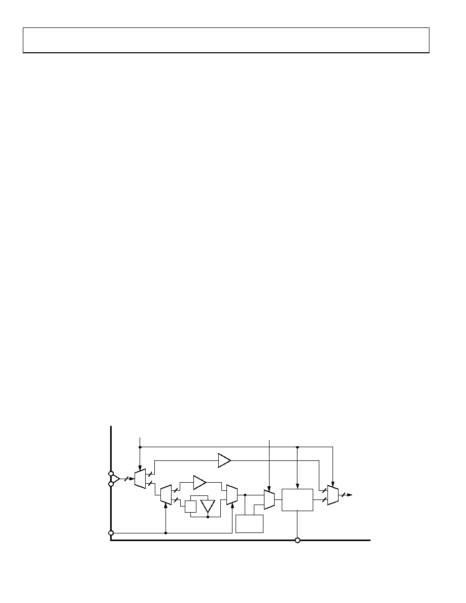
SYSCLK INPUTS
Functional Description
An external time base connects to the AD9912 at the SYSCLK
pins to generate the internal high frequency system clock (fS).
The SYSCLK inputs can be operated in one of the following
three modes:
SYSCLK PLL bypassed
SYSCLK PLL enabled with input signal generated externally
Crystal resonator with SYSCLK PLL enabled
A functional diagram of the system clock generator is shown in
The SYSCLK PLL multiplier path is enabled by a Logic 0 (default)
in the PD SYSCLK PLL bit (Register 0x0010, Bit 4) of the I/O
register map. The SYSCLK PLL multiplier can be driven from
the SYSCLK input pins by one of two means, depending on the
logic level applied to the 1.8 V CMOS CLKMODESEL pin.
When CLKMODESEL = 0, a crystal can be connected directly
across the SYSCLK pins. When CLKMODESEL = 1, the
maintaining amp is disabled, and an external frequency source
(such as an oscillator or signal generator) can be connected
directly to the SYSCLK input pins. Note that CLKMODESEL = 1
does not disable the system clock PLL.
The maintaining amp on the AD9912 SYSCLK pins is intended
for 25 MHz, 3.2 mm × 2.5 mm AT cut fundamental mode crystals
with a maximum motional resistance of 100 Ω. The following
crystals, listed in alphabetical order, meet these criteria (as of
the revision date of this data sheet):
AVX/Kyocera CX3225SB
ECS ECX-32
Epson/Toyocom TSX-3225
Fox FX3225BS
NDK NX3225SA
Note that although these crystals meet the preceding criteria
according to their data sheets, Analog Devices, Inc., does not
guarantee their operation with the AD9912, nor does Analog
Devices endorse one supplier of crystals over another.
When the SYSCLK PLL multiplier path is disabled, the AD9912
must be driven by a high frequency signal source (250 MHz to
1 GHz). The signal thus applied to the SYSCLK input pins becomes
the internal DAC sampling clock (fS) after passing through an
internal buffer.
It is important to note that when bypassing the system clock
PLL, the LOOP_FILTER pin (Pin 31) should be pulled down to
the analog ground with a 1 kΩ resistor.
SYSCLK PLL Doubler
The SYSCLK PLL multiplier path offers an optional SYSCLK
PLL doubler. This block comes before the SYSCLK PLL
multiplier and acts as a frequency doubler by generating a pulse
on each edge of the SYSCLK input signal. The SYSCLK PLL
multiplier locks to the falling edges of this regenerated signal.
The impetus for doubling the frequency at the input of the
SYSCLK PLL multiplier is that an improvement in overall phase
noise performance can be realized. The main drawback is that
the doubler output is not a rectangular pulse with a constant
duty cycle even for a perfectly symmetric SYSCLK input signal.
This results in a subharmonic appearing at the same frequency
as the SYSCLK input signal, and the magnitude of the subharmonic
can be quite large. When employing the doubler, care must be
taken to ensure that the loop bandwidth of the SYSCLK PLL
multiplier adequately suppresses the subharmonic.
The benefit offered by the doubler depends on the magnitude
of the subharmonic, the loop bandwidth of the SYSCLK PLL
multiplier, and the overall phase noise requirements of the
specific application. In many applications, the AD9912 clock
output is applied to the input of another PLL, and the subhar-
monic is often suppressed by the relatively narrow bandwidth of
the downstream PLL.
Note that generally, the benefits of the SYSCLK PLL doubler are
realized for SYSCLK input frequencies of 25 MHz and above.
06
76
3-
03
6
1
0
1
0
1
0
BIPOLAR
EDGE
DETECTOR
2
WITH CRYSTAL
RESONATOR
2
1
0
2
SYSCLK
PLL
ENABLED
WITH EXTERNAL DRIVE
SYSCLK PLL BYPASSED
SYSCLK
PLL
MULTIPLIER
1
0
BIPOLAR EDGE DETECTOR
(I/O REGISTER BIT)
PD SYSCLK PLL
(I/O REGISTER BIT)
DAC
SAMPLE
CLOCK
LOOP_FILTER
SYSCLK
SYSCLKB
CLKMODESEL
2
Figure 44. System Clock Generator Block Diagram
相关PDF资料 |
PDF描述 |
|---|---|
| VI-BWM-IX-B1 | CONVERTER MOD DC/DC 10V 75W |
| VE-22Z-IW-F3 | CONVERTER MOD DC/DC 2V 40W |
| MCF51AC256ACFUE | MCU 32BIT 256K FLASH CAN 64-QFP |
| VE-22Y-IY-F1 | CONVERTER MOD DC/DC 3.3V 33W |
| MK20DX128VFM5 | IC ARM CORTEX MCU 128KB 32LQFN |
相关代理商/技术参数 |
参数描述 |
|---|---|
| AD9912BCPZ | 制造商:Analog Devices 功能描述:Direct Digital Synthesizer 1000MHz 1-DAC 14-Bit Serial 64-Pin LFCSP EP 制造商:Analog Devices 功能描述:DIRECT DGTL SYNTHESIZER 64LFCSP EP - Trays 制造商:Analog Devices 功能描述:IC DDS 1GSPS 14BIT DAC |
| AD9912BCPZ-REEL7 | 制造商:Analog Devices 功能描述:DIRECT DGTL SYNTHESIZER 64LFCSP EP - Tape and Reel |
| AD9913 | 制造商:AD 制造商全称:Analog Devices 功能描述:Low Power 250 MSPS 10-Bit DAC 1.8 V CMOS Direct Digital Synthesizer |
| AD9913/PCBZ | 功能描述:数据转换 IC 开发工具 Sub 50mW 250MSPS (+) 10-bit DDS RoHS:否 制造商:Texas Instruments 产品:Demonstration Kits 类型:ADC 工具用于评估:ADS130E08 接口类型:SPI 工作电源电压:- 6 V to + 6 V |
| AD9913/PCBZ1 | 制造商:AD 制造商全称:Analog Devices 功能描述:Low Power 250 MSPS 10-Bit DAC 1.8 V CMOS Direct Digital Synthesizer |
发布紧急采购,3分钟左右您将得到回复。