- 您现在的位置:买卖IC网 > PDF目录10979 > AD9913BCPZ (Analog Devices Inc)IC DDS 10BIT DAC 250MSPS 32LFCSP PDF资料下载
参数资料
| 型号: | AD9913BCPZ |
| 厂商: | Analog Devices Inc |
| 文件页数: | 10/32页 |
| 文件大小: | 0K |
| 描述: | IC DDS 10BIT DAC 250MSPS 32LFCSP |
| 产品培训模块: | Direct Digital Synthesis Tutorial Series (1 of 7): Introduction Direct Digital Synthesizer Tutorial Series (7 of 7): DDS in Action Direct Digital Synthesis Tutorial Series (3 of 7): Angle to Amplitude Converter Direct Digital Synthesis Tutorial Series (6 of 7): SINC Envelope Correction Direct Digital Synthesis Tutorial Series (4 of 7): Digital-to-Analog Converter Direct Digital Synthesis Tutorial Series (2 of 7): The Accumulator |
| 标准包装: | 1 |
| 分辨率(位): | 10 b |
| 主 fclk: | 250MHz |
| 调节字宽(位): | 32 b |
| 电源电压: | 1.8V |
| 工作温度: | -40°C ~ 85°C |
| 安装类型: | 表面贴装 |
| 封装/外壳: | 32-VFQFN 裸露焊盘,CSP |
| 供应商设备封装: | 32-LFCSP-VQ(5x5) |
| 包装: | 托盘 |
| 产品目录页面: | 552 (CN2011-ZH PDF) |
第1页第2页第3页第4页第5页第6页第7页第8页第9页当前第10页第11页第12页第13页第14页第15页第16页第17页第18页第19页第20页第21页第22页第23页第24页第25页第26页第27页第28页第29页第30页第31页第32页
AD9913
Rev. A | Page 18 of 32
CLOCK INPUT (REF_CLK)
REF_CLK OVERVIEW
The AD9913 supports a number of options for producing the
internal SYSCLK signal (that is, the DAC sample clock) via the
REF_CLK input pins. The REF_CLK input can be driven
directly from a differential or single-ended source, or it can
accept a crystal connected across the two input pins. There is
also an internal phase-locked loop (PLL) multiplier that can be
independently enabled. The various input configurations are
controlled by means of the control bits in the CFR2 [7:5]
register.
Table 6. Clock Input Mode Configuration
CFR2 [7:5]
Mode Configuration
000
Differential Input, PLL Enabled
001
Differential Input, PLL Disabled (Default)
XTAL Input, PLL Enabled
XTAL Input, PLL Disabled
100
CMOS Input, PLL Enabled
101
CMOS Input PLL Disabled
1 x = don’t care.
XTAL
REF_CLK
CMOS
1
0
1
0
10
00
1
0
1
0
÷2
PLL
CFR2[5]
CFR2[6]
DI
V
ID
E
C
O
NT
RO
L
CFR2[5:0]
CFR2[14:9]
DIFFERENTIAL/
SINGLE
CFR2[15]
CFR2[3]
CFR2[7:6]
13
14
SYSTEM
CLOCK
0700
2-
020
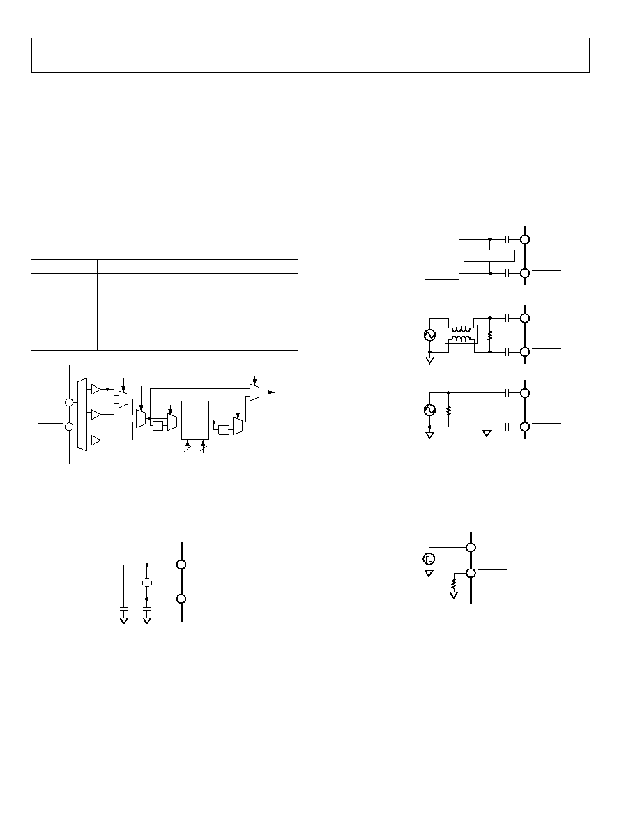
Figure 26. Internal Clock Path Functional Block Diagram
CRYSTAL-DRIVEN REF_CLK
When using a crystal at the REF_CLK input, the resonant
frequency should be approximately 25 MHz. Figure 27 shows
the recommended circuit configuration.
REFCLK
39pF
XTAL
13
14
07
00
2-
0
21
Figure 27. Crystal Connection Diagram
DIRECT-DRIVEN REF_CLK
When driving the REF_CLK inputs directly from a signal
source, either single-ended or differential signals can be used.
With a differential signal source, the REF_CLK pins are driven
with complementary signals and ac-coupled with 0.1 μF
capacitors. With a single-ended signal source, either a single-
ended-to-differential conversion can be employed or the
REF_CLK input can be driven single-ended directly. In either
case, 0.1 μF capacitors are used to ac couple both REF_CLK
pins to avoid disturbing the internal dc bias voltage of ~1.35 V.
See Figure 28 for more details.
The REF_CLK input resistance is ~2.7 kΩ differential (~1.35 kΩ
single-ended). Most signal sources have relatively low output
impedances. The REF_CLK input resistance is relatively high,
therefore, its effect on the termination impedance is negligible
and can usually be chosen to be the same as the output imped-
ance of the signal source. The bottom two examples in Figure 28
assume a signal source with a 50 Ω output impedance.
TERMINATION
REF_CLK
DIFFERENTIAL SOURCE,
DIFFERENTIAL INPUT
SINGLE-ENDED SOURCE,
DIFFERENTIAL INPUT
SINGLE-ENDED SOURCE,
SINGLE-ENDED INPUT
13
14
0.1F
LVPECL,
OR
LVDS
DRIVER
REF_CLK
13
14
50
0.1F
BALUN
(1:1)
REF_CLK
13
14
0.1F
50
07
00
2-
0
22
Figure 28. Direct Connection Diagram
CMOS-DRIVEN REF_CLK
This mode is enabled by writing CFR2 [7] to be true. In this
state, the AD9913 must be driven at Pin 13 with the reference
clock source. Additionally, it is recommended that Pin 14 in
CMOS mode be tied to ground through a 10 kΩ resistor.
13
14
REF_CLK
10k
CMOS
DRIVER
0
70
02
-02
3
Figure 29. CMOS-Driven Diagram
PHASE-LOCKED LOOP (PLL) MULTIPLIER
An internal phase-locked loop (PLL) provides users of the
AD9913 the option to use a reference clock frequency that is
lower than the system clock frequency. The PLL supports a wide
range of programmable frequency multiplication factors (1× to
64×). See Table 7 for details on configuring the PLL multipli-
cation factor. The PLL is also equipped with a PLL_LOCK bit.
CFR2 [15:8] and CFR2 [5:1] control the PLL operation. Upon
power-up, the PLL is off. To initialize the PLL, CFR2 [5] must
be cleared and CFR2 [1] must be set. The function of CFR2 [1]
相关PDF资料 |
PDF描述 |
|---|---|
| MCF51JE128CMB | IC MCU 128K COLDF 81-PBGA |
| AD5930YRUZ | IC GEN PROG FREQ BURST 20TSSOP |
| S9S12HY64J0MLL | MCU 64K FLASH AUTO 100-LQFP |
| VI-21K-CU-S | CONVERTER MOD DC/DC 40V 200W |
| VI-21J-CU-S | CONVERTER MOD DC/DC 36V 200W |
相关代理商/技术参数 |
参数描述 |
|---|---|
| AD9913BCPZ1 | 制造商:AD 制造商全称:Analog Devices 功能描述:Low Power 250 MSPS 10-Bit DAC 1.8 V CMOS Direct Digital Synthesizer |
| AD9913BCPZ-REEL7 | 功能描述:IC DDS 250MSPS 10BIT ADC 32LFCSP RoHS:是 类别:集成电路 (IC) >> 接口 - 直接数字合成 (DDS) 系列:- 产品变化通告:Product Discontinuance 27/Oct/2011 标准包装:2,500 系列:- 分辨率(位):10 b 主 fclk:25MHz 调节字宽(位):32 b 电源电压:2.97 V ~ 5.5 V 工作温度:-40°C ~ 85°C 安装类型:表面贴装 封装/外壳:16-TSSOP(0.173",4.40mm 宽) 供应商设备封装:16-TSSOP 包装:带卷 (TR) |
| AD9913BCPZ-REEL71 | 制造商:AD 制造商全称:Analog Devices 功能描述:Low Power 250 MSPS 10-Bit DAC 1.8 V CMOS Direct Digital Synthesizer |
| AD9914 | 制造商:AD 制造商全称:Analog Devices 功能描述:3.5 GSPS Direct Digital Synthesizer with 12-Bit DAC |
| AD9914/PCBZ | 功能描述:数据转换 IC 开发工具 3.5 GSPS DDS w/Upconverter eval bd. RoHS:否 制造商:Texas Instruments 产品:Demonstration Kits 类型:ADC 工具用于评估:ADS130E08 接口类型:SPI 工作电源电压:- 6 V to + 6 V |
发布紧急采购,3分钟左右您将得到回复。