- 您现在的位置:买卖IC网 > PDF目录10979 > AD9913BCPZ (Analog Devices Inc)IC DDS 10BIT DAC 250MSPS 32LFCSP PDF资料下载
参数资料
| 型号: | AD9913BCPZ |
| 厂商: | Analog Devices Inc |
| 文件页数: | 15/32页 |
| 文件大小: | 0K |
| 描述: | IC DDS 10BIT DAC 250MSPS 32LFCSP |
| 产品培训模块: | Direct Digital Synthesis Tutorial Series (1 of 7): Introduction Direct Digital Synthesizer Tutorial Series (7 of 7): DDS in Action Direct Digital Synthesis Tutorial Series (3 of 7): Angle to Amplitude Converter Direct Digital Synthesis Tutorial Series (6 of 7): SINC Envelope Correction Direct Digital Synthesis Tutorial Series (4 of 7): Digital-to-Analog Converter Direct Digital Synthesis Tutorial Series (2 of 7): The Accumulator |
| 标准包装: | 1 |
| 分辨率(位): | 10 b |
| 主 fclk: | 250MHz |
| 调节字宽(位): | 32 b |
| 电源电压: | 1.8V |
| 工作温度: | -40°C ~ 85°C |
| 安装类型: | 表面贴装 |
| 封装/外壳: | 32-VFQFN 裸露焊盘,CSP |
| 供应商设备封装: | 32-LFCSP-VQ(5x5) |
| 包装: | 托盘 |
| 产品目录页面: | 552 (CN2011-ZH PDF) |
第1页第2页第3页第4页第5页第6页第7页第8页第9页第10页第11页第12页第13页第14页当前第15页第16页第17页第18页第19页第20页第21页第22页第23页第24页第25页第26页第27页第28页第29页第30页第31页第32页
AD9913
Rev. A | Page 22 of 32
I/O PROGRAMMING
SERIAL PROGRAMMING
The AD9913 serial port is a flexible, synchronous serial
communications port allowing an easy interface to many
industry standard microcontrollers and microprocessors.
The interface allows read/write access to all registers that
configure the AD9913. MSB first or LSB first transfer formats
are supported. The AD9913 serial interface port is configured
as a single pin I/O (SDIO), which allows a two-wire interface.
The AD9913 does not have a SDO pin for 3-wire operation.
With the AD9913, the instruction byte specifies read/write
operation and the register address. Serial operations on the
AD9913 occur only at the register level, not the byte level.
For the AD9913, the serial port controller recognizes the
instruction byte register address and automatically generates
the proper register byte address. In addition, the controller
expects that all bytes of that register are accessed. It is a
requirement that all bytes of a register be accessed during
serial I/O operations.
There are two phases to a communication cycle with the
AD9913. Phase 1 is the instruction cycle, which is the writing of
an instruction byte into the AD9913, coincident with the first
eight SCLK rising edges. The instruction byte provides the
AD9913 serial port controller with information regarding the
data transfer cycle, which is Phase 2 of the communication
cycle. The Phase 1 instruction byte defines whether the
upcoming data transfer is read or write and the serial address of
the register being accessed.
The first eight SCLK rising edges of each communication cycle
are used to write the instruction byte into the AD9913. The
remaining SCLK edges are for Phase 2 of the communication
cycle. Phase 2 is the actual data transfer between the AD9913
and the system controller. The number of bytes transferred
during Phase 2 of the communication cycle is a function of the
register accessed. For example, when accessing the Control
Function Register 2, which is two bytes wide, Phase 2 requires
that two bytes be transferred. If accessing one of the profile
registers, which are six bytes wide, Phase 2 requires that six
bytes be transferred. After transferring all data bytes per the
instruction, the communication cycle is completed.
At the completion of any communication cycle, the AD9913
serial port controller expects the next eight rising SCLK edges
to be the instruction byte of the next communication cycle.
All data input to the AD9913 is registered on the rising edge
of SCLK. All data is driven out of the AD9913 on the falling
operation of serial ports.
The IO_UPDATE transfers the contents of the write sequence
to the active register. See the Register Update (I/O Update)
section.
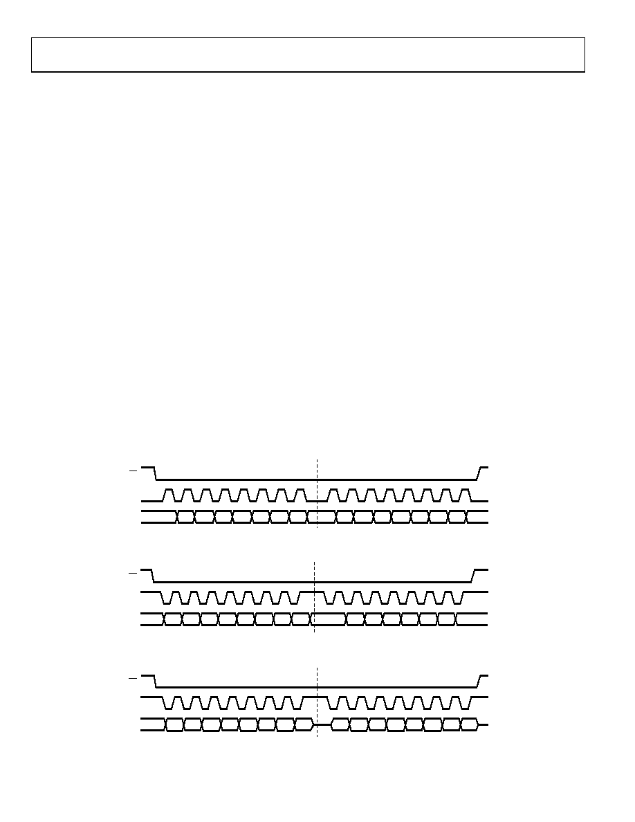
I7
SDIO
INSTRUCTION CYCLE
DATA TRANSFER CYCLE
SCLK
CS
I6
I5
I4
I3
I2
I1
I0
D7
D6
D5
D4
D3
D2
D1
D0
07
00
2-
02
5
Figure 30. Serial Port Writing Timing—Clock Stall Low
I7
SDIO
INSTRUCTION CYCLE
DATA TRANSFER CYCLE
SCLK
CS
I6
I5
I4
I3
I2
I1
I0
D7
D6
D5
D4
D3
D2
D1
D0
07
00
2-
02
6
Figure 31. Serial Port Write Timing—Clock Stall High
I7
SDIO
INSTRUCTION CYCLE
DATA TRANSFER CYCLE
SCLK
CS
I6
I5
I4
I3
I2
I1
I0
DO7
DO6 DO5 DO4 DO3 DO2
DO1 DO0
070
02
-027
Figure 32. Two-Wire Serial Port Read Timing—Clock Stall High
相关PDF资料 |
PDF描述 |
|---|---|
| MCF51JE128CMB | IC MCU 128K COLDF 81-PBGA |
| AD5930YRUZ | IC GEN PROG FREQ BURST 20TSSOP |
| S9S12HY64J0MLL | MCU 64K FLASH AUTO 100-LQFP |
| VI-21K-CU-S | CONVERTER MOD DC/DC 40V 200W |
| VI-21J-CU-S | CONVERTER MOD DC/DC 36V 200W |
相关代理商/技术参数 |
参数描述 |
|---|---|
| AD9913BCPZ1 | 制造商:AD 制造商全称:Analog Devices 功能描述:Low Power 250 MSPS 10-Bit DAC 1.8 V CMOS Direct Digital Synthesizer |
| AD9913BCPZ-REEL7 | 功能描述:IC DDS 250MSPS 10BIT ADC 32LFCSP RoHS:是 类别:集成电路 (IC) >> 接口 - 直接数字合成 (DDS) 系列:- 产品变化通告:Product Discontinuance 27/Oct/2011 标准包装:2,500 系列:- 分辨率(位):10 b 主 fclk:25MHz 调节字宽(位):32 b 电源电压:2.97 V ~ 5.5 V 工作温度:-40°C ~ 85°C 安装类型:表面贴装 封装/外壳:16-TSSOP(0.173",4.40mm 宽) 供应商设备封装:16-TSSOP 包装:带卷 (TR) |
| AD9913BCPZ-REEL71 | 制造商:AD 制造商全称:Analog Devices 功能描述:Low Power 250 MSPS 10-Bit DAC 1.8 V CMOS Direct Digital Synthesizer |
| AD9914 | 制造商:AD 制造商全称:Analog Devices 功能描述:3.5 GSPS Direct Digital Synthesizer with 12-Bit DAC |
| AD9914/PCBZ | 功能描述:数据转换 IC 开发工具 3.5 GSPS DDS w/Upconverter eval bd. RoHS:否 制造商:Texas Instruments 产品:Demonstration Kits 类型:ADC 工具用于评估:ADS130E08 接口类型:SPI 工作电源电压:- 6 V to + 6 V |
发布紧急采购,3分钟左右您将得到回复。