- 您现在的位置:买卖IC网 > PDF目录10979 > AD9953YSVZ (Analog Devices Inc)IC DDS DAC 14BIT 400MSPS 48-TQFP PDF资料下载
参数资料
| 型号: | AD9953YSVZ |
| 厂商: | Analog Devices Inc |
| 文件页数: | 18/32页 |
| 文件大小: | 0K |
| 描述: | IC DDS DAC 14BIT 400MSPS 48-TQFP |
| 产品培训模块: | Direct Digital Synthesis Tutorial Series (1 of 7): Introduction Direct Digital Synthesizer Tutorial Series (7 of 7): DDS in Action Direct Digital Synthesis Tutorial Series (3 of 7): Angle to Amplitude Converter Direct Digital Synthesis Tutorial Series (6 of 7): SINC Envelope Correction Direct Digital Synthesis Tutorial Series (4 of 7): Digital-to-Analog Converter Direct Digital Synthesis Tutorial Series (2 of 7): The Accumulator |
| 标准包装: | 1 |
| 分辨率(位): | 14 b |
| 主 fclk: | 400MHz |
| 调节字宽(位): | 32 b |
| 电源电压: | 1.71 V ~ 1.96 V |
| 工作温度: | -40°C ~ 105°C |
| 安装类型: | 表面贴装 |
| 封装/外壳: | 48-TQFP 裸露焊盘 |
| 供应商设备封装: | 48-TQFP 裸露焊盘(7x7) |
| 包装: | 托盘 |
| 产品目录页面: | 552 (CN2011-ZH PDF) |
第1页第2页第3页第4页第5页第6页第7页第8页第9页第10页第11页第12页第13页第14页第15页第16页第17页当前第18页第19页第20页第21页第22页第23页第24页第25页第26页第27页第28页第29页第30页第31页第32页
AD9953
Rev. A | Page 25 of 32
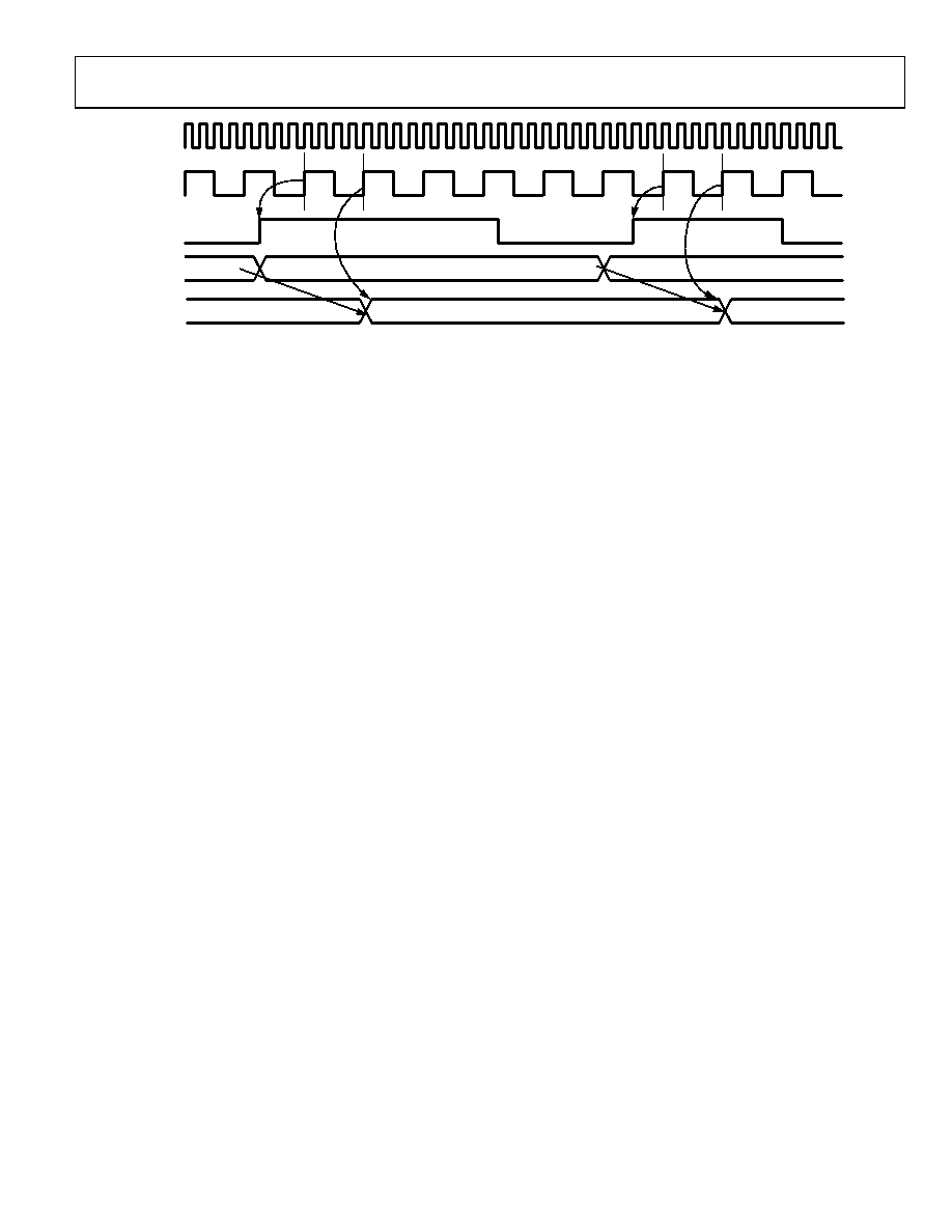
SYSCLK
SYNC_CLK
I/O UPDATE
AB
DATA IN
I/O BUFFERS
DATA 1
DA
DATA IN
REGISTERS
DATA 0
THE DEVICE REGISTERS AN I/O UPDATE AT POINT A.
Figure
AB
TA 2
DATA 3
DATA
THE DATA IS TRANS
22. I/O Synchronization Tim
ser:
ons must be observed. First, all units must share a common
clock source. Trace lengths and path impedance of the clock
tree must be designed to keep the phase delay of the different
clock branches as closely matched as possible. Second, the I/O
UPDATE signal’s rising edge must be provided synchronously
to all devices in the system. Finally, regardless of the internal
synchronization method used, the DVDD_I/O supply should
be set to 3.3 V for all devices that are to be synchronized.
AVDD and DVDD should be left at 1.8 V.
In automatic synchronization mode, one device is chosen as a
master; the other device(s) will be slaved to this master. When
configured in this mode, the slaves will automatically synchron-
ize their internal clocks to the SYNC_CLK output signal of the
master device. To enter automatic synchronization mode, set
the slave device’s automatic synchronization bit (CFR1<23> =
1). Connect the SYNC_IN input(s) to the master SYNC_CLK
output. The slave device will continuously update the phase
relationship of its SYNC_CLK until it is in phase with the
SYNC_IN input, which is the SYNC_CLK of the master device.
When attempting to synchronize devices running at SYSCLK
speeds beyond 250 MSPS, the high speed sync enhancement
enable bit should be set (CFR2<11> = 1).
n software manual synchronization mode, the user forces the
evice to advance the SYNC_CLK rising edge one SYSCLK
ycle (1/4 SYNC_CLK period). To activate the manual
nchronization mode, set the slave device’s software manual
ynchronization bit (CFR1<22> = 1). The bit (CFR1<22>) will be
eared immediately. To advance the rising edge of the SYNC_CLK
ultiple times, this bit will need to be set multiple times.
In h
inpu
configured such that it will now advance the rising
dge of the SYNC_CLK signal each time the device detects a
sing edge on the SYNC_IN pin. To put the device into hard-
are manual synchronization mode, set the hardware manual
synchronization bit (CFR2<10> = 1). Unlike the software
manual synchronization bit, this bit does not self clear. Once the
hardware manual synchronization mode is enabled, all rising
edges detected on the SYNC_IN input will cause the device to
advance the rising edge of the SYNC_CLK by one SYSCLK
cycle until this enable bit is cleared (CFR2<10> = 0).
Using a Single Crystal to Drive Multiple AD9953 Clock
Inputs
The AD9953 crystal oscillator output signal is available on the
CRYSTAL OUT pin, enabling one crystal to drive multiple
AD9953s. In order to drive multiple AD9953s with one crystal,
the CRYSTAL OUT pin of the AD9953 using the external crystal
should be connected to the REFCLK input of the other AD9953.
The CRYSTAL OUT pin is static until the CFR2<9> bit is set,
enabling the output. The drive strength of the CRYSTAL OUT
pin is typically very low, so this signal should be buffered prior
to using it to drive any loads.
SERIAL PORT OPERATION
With the AD9953, the instruction byte specifies read/write
operation and the register address. Serial operations on the
AD9953 occur only at the register level, not the byte level. For
e serial po t controller recognizes the instruc-
tion byte register address and automatically generates the
proper register byte address. In addition, the controller expects
that all bytes of that register will be accessed. It is required that
all bytes of a register be accessed during serial I/O operations,
with one exception. The IOSYNC function can be used to abort
an I/O operation, thereby allowing some, but not all bytes to be
accessed.
1
DATA 2
FERRED FROM THE I/O BUFFERS AT POINT B.
03
35
7-
0
07
ing Diagram
Synchronizing Multiple AD9953s
The AD9953 allows easy synchronization of multiple AD9953s.
There are three modes of synchronization available to the u
an automatic synchronization mode, a software controlled
manual synchronization mode, and a hardware controlled
manual synchronization mode. In all cases, when a user wants
to synchronize two or more devices, the following considera-
ti
I
d
c
sy
s
cl
m
ardware manual synchronization mode, the SYNC_IN
t pin is
e
ri
w
the AD9953, th
r
相关PDF资料 |
PDF描述 |
|---|---|
| VE-2WX-IY-F4 | CONVERTER MOD DC/DC 5.2V 50W |
| DS3174+ | IC TXRX DS3/E3 QUAD 400-BGA |
| DS3173N | IC TRPL DS3/E3 TXRX 400-PBGA |
| AD9830ASTZ | IC DDS 10BIT 50MHZ CMOS 48-TQFP |
| VE-2WW-IY-F4 | CONVERTER MOD DC/DC 5.5V 50W |
相关代理商/技术参数 |
参数描述 |
|---|---|
| AD9953YSVZ-REEL7 | 功能描述:IC DDS DAC 14BIT 1.8V 48TQFP RoHS:是 类别:集成电路 (IC) >> 接口 - 直接数字合成 (DDS) 系列:- 产品变化通告:Product Discontinuance 27/Oct/2011 标准包装:2,500 系列:- 分辨率(位):10 b 主 fclk:25MHz 调节字宽(位):32 b 电源电压:2.97 V ~ 5.5 V 工作温度:-40°C ~ 85°C 安装类型:表面贴装 封装/外壳:16-TSSOP(0.173",4.40mm 宽) 供应商设备封装:16-TSSOP 包装:带卷 (TR) |
| AD9954 | 制造商:AD 制造商全称:Analog Devices 功能描述:400 MSPS 14-Bit, 1.8 V CMOS Direct Digital Synthesizer |
| AD9954/PCB | 制造商:Analog Devices 功能描述:AD9954 400 MSPS DDS W/ 14 BIT DAC EVALBD - Bulk 制造商:Analog Devices 功能描述:EVALUATION KIT ((NS)) |
| AD9954/PCBZ | 功能描述:BOARD EVAL FOR 9954 RoHS:是 类别:编程器,开发系统 >> 评估演示板和套件 系列:AgileRF™ 标准包装:1 系列:PSoC® 主要目的:电源管理,热管理 嵌入式:- 已用 IC / 零件:- 主要属性:- 次要属性:- 已供物品:板,CD,电源 |
| AD9954/PCBZ1 | 制造商:AD 制造商全称:Analog Devices 功能描述:400 MSPS, 14-Bit, 1.8 V CMOS, Direct Digital Synthesizer |
发布紧急采购,3分钟左右您将得到回复。