参数资料
| 型号: | AD9979BCPZRL |
| 厂商: | Analog Devices Inc |
| 文件页数: | 28/56页 |
| 文件大小: | 0K |
| 描述: | IC PROCESSOR CCD 14BIT 48-LFCSP |
| 标准包装: | 1 |
| 类型: | CCD 信号处理器,14 位 |
| 输入类型: | 逻辑 |
| 输出类型: | 逻辑 |
| 接口: | 3 线串口 |
| 电流 - 电源: | 48mA |
| 安装类型: | 表面贴装 |
| 封装/外壳: | 48-VFQFN 裸露焊盘,CSP |
| 供应商设备封装: | 48-LFCSP-VQ(7x7) |
| 包装: | 标准包装 |
| 其它名称: | AD9979BCPZRLDKR |
第1页第2页第3页第4页第5页第6页第7页第8页第9页第10页第11页第12页第13页第14页第15页第16页第17页第18页第19页第20页第21页第22页第23页第24页第25页第26页第27页当前第28页第29页第30页第31页第32页第33页第34页第35页第36页第37页第38页第39页第40页第41页第42页第43页第44页第45页第46页第47页第48页第49页第50页第51页第52页第53页第54页第55页第56页
AD9979
Rev. C | Page 34 of 56
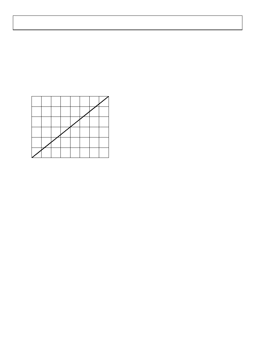
Variable Gain Amplifier (VGA)
The VGA stage provides a gain range of approximately 6 dB to
42 dB, programmable with 10-bit resolution through the serial
digital interface. A gain of 6 dB is needed to match a 1 V input
signal with the ADC full-scale range of 2 V. When compared to
1 V full-scale systems, the equivalent gain range is 0 dB to 36 dB.
The VGA gain curve follows a linear-in-dB characteristic. The
exact VGA gain is calculated for any gain register value by
Gain (dB) = (0.0358 × Code) + 5.75 dB
where Code is the range of 0 to 1023.
VGA GAIN REGISTER CODE
VG
A
GA
IN
(
d
B
)
42
36
30
24
18
12
6
0
127
255
383
511
639
767
895
1023
0
59
57
-05
3
Figure 51. VGA Gain Curve
Analog-to-Digital Converter
The AD9979 uses a high performance ADC architecture,
optimized for high speed and low power. Differential nonlinearity
(DNL) performance is typically better than 0.5 LSB. The ADC
uses a 2 V input range. (See Figure 5 to Figure 7 for the typical
linearity and noise performance plots of the AD9979.)
Optical Black Clamp
The optical black clamp loop is used to remove residual offsets
in the signal chain and to track low frequency variations in the
CCD black level. During the optical black (shielded) pixel
interval on each line, the ADC output is compared with a fixed
black level reference, selected by the user in the clamp level
register. The value can be programmed between 0 LSB and
255 LSB, in 256 steps. The resulting error signal is filtered to
reduce noise, and the correction value is applied to the ADC
input through a DAC. Normally, the optical black clamp loop is
turned on once per horizontal line, but this loop can be updated
more slowly to suit a particular application. If external digital
clamping is used during the postprocessing, the AD9979 optical
black clamping can be disabled using CLAMPENABLE, Bit 3 in
Address 0x00. When the loop is disabled, the clamp level register
can still be used to provide fixed offset adjustment.
Note that if the CLPOB loop is disabled, higher VGA gain settings
reduce the dynamic range because the uncorrected offset in the
signal path is gained up.
It is recommended to align the CLPOB pulse with the CCD
optical black pixels. It is recommended that the CLPOB pulse
duration be at least 20 pixels wide. Shorter pulse widths can be
used, but the ability for the loop to track low frequency variations
in the black level is reduced. See the Horizontal Clamping and
Blanking section for more timing information.
Digital Data Outputs
The AD9979 digital output data is latched using the DOUTPHASEx
value, as shown in Figure 42. (Output data timing is shown
in Figure 20.) The switching of the data outputs can couple
noise back into the analog signal path. To minimize any switching
noise while using default register settings, it is recommended
that DOUTPHASEPx be set to a value between 15 and 31. Other
settings can produce good results, but experimentation is
necessary.
The data output coding is normally straight binary, but the coding
can be changed to gray coding by setting Bit 2 of Address 0x01 to 1.
相关PDF资料 |
PDF描述 |
|---|---|
| AD9980KSTZ-95 | IC INTERFACE 8BIT ANALOG 80LQFP |
| AD9981KSTZ-95 | IC INTERFACE 10BIT ANALOG 80LQFP |
| AD9983AKSTZ-170 | IC DISPLAY 8BIT 170MSPS 80LQFP |
| AD9985KSTZ-140 | IC INTERFACE 8BIT 140MSPS 80LQFP |
| AD9990BBCZ | IC CCD SGNL PROCESSOR 112CSPBGA |
相关代理商/技术参数 |
参数描述 |
|---|---|
| AD9980 | 制造商:AD 制造商全称:Analog Devices 功能描述:High Performance 8-Bit Display Interface |
| AD9980/PCBZ | 功能描述:KIT EVALUATION AD9980 RoHS:是 类别:编程器,开发系统 >> 评估演示板和套件 系列:Advantiv® 标准包装:1 系列:PCI Express® (PCIe) 主要目的:接口,收发器,PCI Express 嵌入式:- 已用 IC / 零件:DS80PCI800 主要属性:- 次要属性:- 已供物品:板 |
| AD9980KSTZ-80 | 功能描述:IC INTERFACE 8BIT ANALOG 80LQFP RoHS:是 类别:集成电路 (IC) >> 接口 - 专用 系列:- 特色产品:NXP - I2C Interface 标准包装:1 系列:- 应用:2 通道 I²C 多路复用器 接口:I²C,SM 总线 电源电压:2.3 V ~ 5.5 V 封装/外壳:16-TSSOP(0.173",4.40mm 宽) 供应商设备封装:16-TSSOP 包装:剪切带 (CT) 安装类型:表面贴装 产品目录页面:825 (CN2011-ZH PDF) 其它名称:568-1854-1 |
| AD9980KSTZ-95 | 功能描述:IC INTERFACE 8BIT ANALOG 80LQFP RoHS:是 类别:集成电路 (IC) >> 接口 - 专用 系列:- 特色产品:NXP - I2C Interface 标准包装:1 系列:- 应用:2 通道 I²C 多路复用器 接口:I²C,SM 总线 电源电压:2.3 V ~ 5.5 V 封装/外壳:16-TSSOP(0.173",4.40mm 宽) 供应商设备封装:16-TSSOP 包装:剪切带 (CT) 安装类型:表面贴装 产品目录页面:825 (CN2011-ZH PDF) 其它名称:568-1854-1 |
| AD9980KSTZ-RL95 | 制造商:Analog Devices 功能描述: |
发布紧急采购,3分钟左右您将得到回复。